
Why UPW Defines Yield in a US Chip Fab
Ultra pure water (UPW) is the single largest process chemical by volume in any 300 mm fab, used as a cleaning agent, diluent, etchant carrier, and final rinse across hundreds of wet bench steps (per IEEE ASMC 2016, S1). Because UPW contacts every wafer multiple times between photo, etch, and CMP, its quality directly determines whether a die survives the line: one particle event at the wrong step can scrap an entire lot. As production migrates to 3 nm and 2 nm nodes, the contamination budget has tightened from parts-per-billion to parts-per-trillion for trace metals, dissolved silica, and total organic carbon (TOC). Market forecasts put the global UPW-for-semiconductor segment at a 13.9% CAGR from 2026 to 2033, with the US capturing roughly 35% of that spend (per the 2026–2033 UPW market outlook, S4). The practical consequence for a process engineer is straightforward: design capacity follows purity, not the other way around.
The 2026 UPW Contamination Budget: ASTM D5127 and SEMI F63 Limits
The binding 2026 specification for advanced-node fabs is anchored in ASTM D5127 (Standard Guide for UPW in Electronics) and SEMI F63 (UPW for Semiconductor Processing), which define the contamination budget the polishing loop must deliver. The headline targets are 18.2 MΩ·cm resistivity at 25 °C, <1 ppb TOC, <1 ppt dissolved silica, and <1 ppt each for critical trace metals including Cu, Fe, Na, and K (per S5 pilot confirmation of 18.2 MΩ·cm and <1 ppb DOC on reclaimed RO permeate). Particle counts must stay below 1 particle/L at ≥50 nm for sub-3 nm work, and bacterial counts below 1 CFU/L, typically achieved by 185/254 nm UV paired with a nitrogen blanket and periodic hot-water sanitization (per the UPW microbial-control discussion in S3, 2014). Market data segment operational practice into Above 18 MΩ·cm for critical wet benches and Below 18 MΩ·cm for non-critical rinsing (per S4).
| Parameter | 2026 Target (ASTM D5127 / SEMI F63) | Typical Unit Operation Responsible |
|---|---|---|
| Resistivity at 25 °C | 18.2 MΩ·cm | Mixed-bed polish, EDI |
| TOC / DOC | <1 ppb | 185/254 nm UV, mixed-bed |
| Dissolved silica | <1 ppt | Two-stage RO, mixed-bed |
| Trace metals (Cu, Fe, Na, K) | <1 ppt each | Two-stage RO, EDI, mixed-bed |
| Particles ≥50 nm | <1 /L | UF, sub-micron final filter |
| Bacteria | <1 CFU/L | UV (254 nm), N2 blanket, periodic hot sanitization |
| ORP | Reducing | N2 blanket, ORP-controlled polish |
Reference Treatment Train: From City Water to Polishing Loop
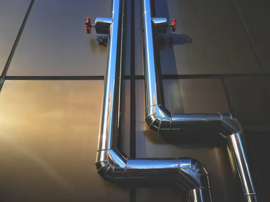
A 2026 US fab UPW train consists of five distinct stages, each with a defined duty and a measurable effluent target.
- Pretreatment. Multimedia filtration drops turbidity, activated carbon strips free chlorine and organics, and a water softener reduces hardness to keep the RO Silt Density Index below 3.
- Primary purification. A two-pass reverse osmosis (RO) train targets >75% overall system recovery. The 2nd-stage RO is operated intermittently to balance recovery against membrane fouling, a control strategy directly validated in the S5 pilot (2025). A PVDF ultrafiltration skid ahead of the train removes colloids and large macromolecules; integrity is verified by periodic pressure-hold testing because particle monitoring alone is insufficient for detecting pinhole and fiber breaks (per S1, IEEE ASMC 2016).
- Polishing. A continuous electrodeionization stack lifts RO permeate into the 17–18 MΩ·cm range without acid or caustic regeneration, simplifying chemical handling and waste.
- Final polish. A non-regenerable mixed-bed ion exchanger drives the train to 18.2 MΩ·cm; a sub-micron final filter catches any downstream particle shedding; 185/254 nm UV oxidizes residual TOC to sub-ppb levels and controls microbial growth.
- Storage and distribution. The loop is electropolished 304L/316L, N2-blanketed to keep ORP reducing, and instrumented with online TOC, resistivity, particle, and ORP analyzers tied to the fab's data historian.
This sequence matches the contamination budget row-for-row: RO and EDI carry the ionic load, mixed-bed and UV carry the trace ionic and organic load, and the storage/distribution loop prevents recontamination between the central plant and point-of-use.
Closing the Loop: Reuse of Semiconductor Wastewater as UPW Feed
CHIPS Act siting in Arizona, Texas, and Ohio is forcing every new fab to answer the same water question: where does the UPW intake come from, and how much of it can be reclaimed? A 2025 pilot integrating UF with two-stage RO on real fab wastewater demonstrated >75% recovery and 0.5 mgC/L DOC in the RO permeate, with the lab-scale UPW polish on that permeate consistently producing ≥18.2 MΩ·cm resistivity and <1 ppb DOC (per S5). The same study flagged the residual foulants that 2026 designs must target: low-MW neutral species such as urea, and metal-humic complexes carrying Cr2+ and Ni2+. PFAS and tetramethylammonium hydroxide (TMAH) developer chemicals are the additional 2026 pretreatment priorities, with direct implications for carbon selection (high-capacity virgin carbon, not just reactivated) and RO staging (intermittent 2nd-pass to manage biofouling). The pilot's economic analysis concluded that, although UF and two-stage RO add CAPEX and OPEX, the reuse loop is strategically viable because supply security in water-stressed US counties outweighs the operating penalty. Engineers evaluating reuse should pilot on-site for at least one quarter of normal flow before locking the train design, with sampling targeted at the low-MW neutral and metal-humic fractions S5 identified.
Equipment Selection Criteria for UPW Skids
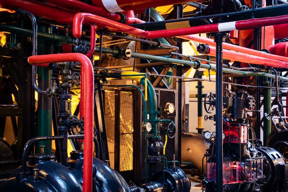
Translating the contamination budget into a shortlist requires asking the right questions of every vendor and verifying the answers against a written specification.
| Unit | Must-Ask Specification | Why It Matters |
|---|---|---|
| UF membrane | PVDF vs PES, nominal pore size, pressure-hold test frequency | Determines colloid removal and whether integrity testing is built into O&M (per S1) |
| RO membranes | Feed spacer thickness, fouling-resistant coating, recovery curve, intermittent 2nd-stage capability | Recovery >75% and fouling control under intermittent 2nd-pass operation (per S5) |
| EDI stack | Current density range, resin grade, module voltage limit | Sustains 17–18 MΩ·cm without chemical regeneration |
| Mixed-bed | Resin grade (nuclear-grade vs semiconductor-grade), rinse-up volume, replacement cycle | Drives final 18.2 MΩ·cm and trace-metal removal |
| UV | 185/254 nm combined, dose at design flow, lamp life | TOC oxidation to <1 ppb and microbial control |
| Instrumentation | Online TOC, resistivity, ≥50 nm particle counter, ORP | Must be in the scope of supply, not an afterthought |
The 2026 supply base spans membrane and resin OEMs (Dow, Mitsubishi Chemical, Purolite, Organo, Sunresin) and systems houses (Evoqua, SUEZ), with HydropureWater positioned as a skid integrator that combines these technologies into packaged units. Routine UF integrity testing via the pressure-hold method should be written into the procurement document as an O&M deliverable (per S1). For consumables planning, factory-stock RO and UF membrane replacements and a 185/254 nm TOC-reduction UV sized to the design flow should be included on the spares list at commissioning.
Cost Snapshot: What a 300 mm Fab UPW System Runs in 2026
For sanity-checking vendor quotes, the order-of-magnitude envelope is well established: a 300 mm fab UPW train typically lands in the low-to-mid single-digit millions USD for the central system, with the total fab water treatment envelope (pretreatment, reclaim, polishing, distribution, and waste treatment) running several multiples higher. The dominant cost drivers are RO staging and membrane replacement, mixed-bed resin change-out cadence, EDI stack replacement at end of service life, and the energy for high-pressure RO pumps plus continuous UV lamp operation. Industrial water tariffs in Arizona, Texas, and Ohio are rising faster than the historical baseline, which converts any reuse loop into a measurable OPEX hedge. The detailed CAPEX/OPEX/ROI breakdown for 2026 is laid out in the 2026 cost guide for 300 mm fab UPW systems.
Frequently Asked Questions
What resistivity is required for semiconductor UPW?
Advanced-node fabs target 18.2 MΩ·cm at 25 °C, with <1 ppb TOC and <1 ppt trace metals per ASTM D5127 and SEMI F63. Critical wet benches run at the 18.2 MΩ·cm spec, while non-critical rinsing can operate below 18 MΩ·cm (per S4).
Why is UF used in UPW systems?
UF removes colloids, particles, and large macromolecules upstream of the polishing loop. Because particle monitoring alone misses pinholes and fiber breaks, periodic pressure-hold integrity testing is required as a complementary quality-control measure (per IEEE ASMC 2016, S1).
Can semiconductor wastewater be reused for UPW?
Yes. A pilot-scale UF + two-stage RO system on real fab wastewater achieved >75% recovery and 0.5 mgC/L DOC, and the RO permeate consistently produced ≥18.2 MΩ·cm and <1 ppb DOC at lab-scale polish, confirming it as a viable UPW intake source (per S5, 2025).
How much does a fab UPW system cost in 2026?
The order-of-magnitude is low-to-mid single-digit millions USD for a 300 mm fab UPW train, with the total fab water treatment envelope substantially higher. The full breakdown is in the 2026 cost guide for 300 mm fab UPW systems.
Which standards govern UPW quality in 2026?
ASTM D5127 and SEMI F63 set the contamination budget for resistivity, TOC, silica, metals, particles, and bacteria. The complete parameter set is in the 2026 UPW contamination budget guide.
Related Equipment
- PVDF ultrafiltration skid — specifications, capacity range, and technical data