Semiconductor UPW plant design under SEMI F63 must deliver resistivity above 18.2 MΩ·cm at 25°C, TOC below 1 ppb, and particles below 1/mL at 0.05 µm, because silica breakthrough or biofilm can cut wafer yields by 5–15% at 3nm and smaller nodes.
Advanced fabs use 2–4 million gallons of UPW daily. According to Wikipedia's ultrapure water overview, advanced fabrication plants consume several million gallons of UPW per day, and some now feed reclaimed wastewater into the front of the train. Costs concentrate in pretreatment with RO recovery up to 95%, polishing by EDI or DI, and continuous loop monitoring.
Semiconductor Ultrapure Water System Specifications for Fabs: What Protects Purity and Reliability?
A 2026 semiconductor UPW plant is an engineered train that converts feed water into fab-grade ultrapure water through pretreatment, high-rejection RO, polishing, UV oxidation, and circulating distribution. Design targets fixed purity limits, continuous online monitoring, and redundant polishing so ionic, organic, particle, and microbial excursions do not reach process tools.
Contamination events can cost fabs $50K–$200K per incident in downtime and scrap wafers, as documented by SEMI E157-1120. One major manufacturer saw a 5% yield loss in a 28nm plant after silica exceeded 0.5 ppb in the polishing loop. Exhausted mixed-bed DI resin that missed regeneration allowed dissolved silica into the final supply.
In another case, a 12% rise in CMP defects tracked TOC spikes above 2 ppb from biofilm in distribution piping. The fab needed a 3-day shutdown for sanitization and loop re-passivation. Organic films leave residues that disrupt later process steps and device performance.
Purity targets tighten with each node. A 14nm fab may hold TOC below 1 ppb, while 5nm and smaller lines often require TOC below 0.5 ppb. Missed limits raise defect density, cut yield, and inflate scrap cost for advanced nodes.
Particle logic scales the same way. According to Wikipedia's ultrapure water overview, particles must be filtered down to a 'critical particle size' that is one-half of the smallest feature size on a semiconductor chip. For 40 nm features, all particles above 20 nm (0.02 μm) are removed, and distribution filters with pore sizes ≤200 nm back up that rule at the point of use.
SEMI F63-0921 Ultrapure Water Quality Limits and Compliance Testing
The F63-0921 document sets the UPW quality envelope used for system design and day-to-day compliance. Online analyzers and scheduled grab samples confirm that process water does not add ionic, organic, particulate, or microbial load to wafers. Resistivity alone is not enough, because organics and uncharged silica barely move conductivity yet still create yield loss.
Online TOC analyzers resolve organics near 0.1 ppb. Laser particle counters quantify particles down to 0.05 µm. The 2021 update tightened boron to <0.05 ppb and germanium to <0.1 ppb for EUV lithography. A high-recovery RO system for semiconductor UPW plants removes bulk dissolved solids before polishing stages finalize the loop.
Historical context frames the tightening. According to Wikipedia's ultrapure water overview, as of 2002, 1–2 parts of contaminating molecules per one million water molecules was considered ultrapure water. The F63-0921 table now works far below that mark on every ionic and organic parameter, which is why online analytics carry so much of the compliance burden.
| Parameter | SEMI F63-0921 Limit | Typical Measurement Method | Relevance to Fab Performance |
|---|---|---|---|
| Resistivity | >18.2 MΩ·cm @ 25°C | Online conductivity meter | Indicates ionic purity; critical for wet cleans & etching. |
| Total Organic Carbon (TOC) | <1 ppb (0.5 ppb for <5nm nodes) | Online UV/persulfate TOC analyzer | Prevents organic residue deposition, critical for gate oxide integrity. |
| Dissolved Silica | <0.3 ppb (0.05 ppb for <5nm nodes) | Online colorimetric or ICP-MS | Prevents silicate deposition, critical for gate oxide defects. |
| Particles (0.05 µm) | <1/mL | Online laser particle counter | Prevents physical defects on wafer surfaces. |
| Bacteria | <1 CFU/100 mL (0.1 CFU/100 mL for <5nm nodes) | Offline culture or online ATP assay | Prevents biofilm formation & organic contamination. |
| Dissolved Oxygen | <10 ppb | Online DO sensor | Prevents oxidation of sensitive materials. |
| Metals (e.g., Fe, Cu, Na) | <0.01 ppb each | ICP-MS (grab sample) | Prevents metallic contamination, impacting device electrical properties. |
| Boron | <0.05 ppb (for EUV) | ICP-MS (grab sample) | Specific concern for advanced lithography. |
| Germanium | <0.1 ppb (for EUV) | ICP-MS (grab sample) | Specific concern for advanced lithography. |
Semiconductor UPW Plant Design Under SEMI F63: Process Flow and Unit Operations
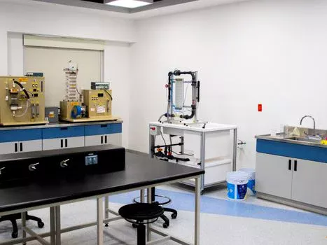
Pretreatment protects downstream membranes and resins. Multi-media filters remove suspended solids, softeners cut calcium and magnesium, and activated carbon adsorbs chlorine plus larger organics. Primary purification then uses a 2-stage RO train at 75–85% recovery to strip dissolved salts before intermediate storage.
Polishing with EDI or mixed-bed DI pushes resistivity above 18 MΩ·cm. EDI typically recovers 90–95% of feed, but feed SDI must stay below 3 and hardness below 1 ppm to limit membrane scale. UV at 185 nm breaks residual organics into ionizable fragments, while 254 nm UV provides disinfection. Final 0.05 µm filtration precedes the circulating distribution loop.
EDI's placement after RO is structural, not optional. Wikipedia's electrodeionization overview describes EDI as typically employed as a polishing treatment following reverse osmosis, because the modules tolerate only low-TDS feed. Feed hardness is 'often limited to 1 part per million (ppm) of CaCO3', and silica 'generally must be no more than 1 ppm in most EDI cells or 2 ppm in thin-cell modules'. Those limits are why softening and degassing sit between RO and EDI on every train we build.
Integrated water purification systems combine these stages in one skid layout, and precision chemical dosing for UPW pretreatment keeps RO feed chemistry stable.
Broader semiconductor high-purity water treatment engineering specs cover adjacent process-water trains on the same fab site.
| Unit Operation | Key Specification/Parameter | Typical Performance/Range | Primary Function | Potential Failure Mode |
|---|---|---|---|---|
| Multi-Media Filter (MMF) | Filtration Rate | 5–10 gpm/ft² | Removes suspended solids >10 µm | Channeling, media fouling, backwash failure |
| Activated Carbon Filter (ACF) | Empty Bed Contact Time (EBCT) | 5–10 minutes | Removes chlorine, chloramines, large organics | Carbon exhaustion, breakthrough of chlorine/organics |
| Reverse Osmosis (RO) | Membrane Type Recovery Rate Salt Rejection |
Polyamide Thin-Film Composite 75–85% (2-stage) >99% |
Removes dissolved salts, organics, colloids | Fouling (scaling, biofouling), membrane damage, permeate quality drop |
| Electrodeionization (EDI) | Module Voltage Recovery Rate Feed Hardness |
200–400 VDC 90–95% <1 ppm |
Removes remaining ionic impurities (polishing) | Scaling, fouling, membrane damage, resistivity drop |
| Mixed-Bed Deionization (DI) | Resin Capacity Flow Rate |
>20,000 grains/ft³ 20–40 gpm/ft³ |
Removes remaining ionic impurities (polishing) | Resin exhaustion, channeling, silica breakthrough |
| UV Oxidation (TOC) | Wavelength UV Dose |
185 nm >200 mJ/cm² |
Breaks down organic molecules | Lamp failure, low UV intensity, incomplete TOC reduction |
| UV Disinfection | Wavelength UV Dose |
254 nm >40 mJ/cm² |
Inactivates bacteria & viruses | Lamp failure, low UV intensity, microbial growth |
| Ultrafine Filtration | Pore Size | 0.05 µm | Removes sub-micron particles | Filter clogging, breakthrough of particles |
Which UPW System Designs Fit CHIPS Act Fab Projects?
Architecture choice among RO+DI, RO+EDI, and hybrid RO+EDI+DI drives CAPEX, footprint, and purity stability. RO+DI usually carries about 20% lower CAPEX than RO+EDI, yet about 30% higher OPEX from resin regeneration near $0.20/m³ versus about $0.05/m³ for EDI. Continuous high-volume fabs therefore favor EDI polishing when feed quality is stable.
RO EDI Polishing for Semiconductor UPW Plant Architectures
RO+EDI suits many 14nm and larger nodes that need steady quality without regeneration downtime. Hybrid RO+EDI+DI adds the highest investment and the strongest contamination buffer for 3nm and smaller nodes or variable feed. EDI typically removes 90–95% of silica; the final DI scavenger takes the remaining 5–10% to sub-ppb levels. See also detailed cost breakdowns for semiconductor UPW treatment systems and semiconductor high-purity water systems cost models.
Designing a Semiconductor UPW Plant for Sub-5nm Node Yield
Sub-5nm yield is where water chemistry shows up on the P&L. A 1 ppb TOC rise has been linked to 0.5–1% yield loss on advanced 5nm nodes, and dissolved silica above 0.3 ppb threatens gate oxide integrity. Hybrid trains with dual polishing and continuous TOC monitoring are the usual answer at this node class, because a single exhausted polisher cannot be tolerated.
| Dimension | RO+DI System | RO+EDI System | Hybrid (RO+EDI+DI) System |
|---|---|---|---|
| CAPEX (Relative) | Low (Baseline) | Medium (+20% vs. RO+DI) | High (+35-50% vs. RO+DI) |
| OPEX (Relative) | High (+30% vs. RO+EDI) | Medium (Baseline) | Medium-High (+10% vs. RO+EDI) |
| Footprint | Medium (requires regeneration skid) | Small (compact modules) | Medium (EDI + smaller DI polisher) |
| TOC Removal | Good (with UV) | Excellent (with UV) | Excellent (with UV) |
| Silica Removal | Excellent (batch process) | Good (90-95% continuous) | Excellent (EDI + DI polisher for trace) |
| Microbial Control | Good (with UV & sanitization) | Excellent (with UV, less biofilm risk) | Excellent (with UV, maximum redundancy) |
| Energy Use (kWh/m³) | 1.0-1.2 | 0.8-1.0 | 0.9-1.1 |
| Maintenance Complexity | High (chemical handling, resin transfers) | Medium (module cleaning, monitoring) | Medium-High (EDI + DI management) |
| Typical Application | Older fabs, smaller fabs, non-critical applications | 14nm+ fabs, stable feed water, sustainability focus | <5nm fabs, variable feed water, low-risk requirement |
Semiconductor UPW Plant CapEx Opex Breakdown: 5-Year TCO
New plant CAPEX typically runs from $2M for a 50 m³/h system to $5M for a 200 m³/h system. About 60% of that spend sits in pretreatment and primary RO, covering equipment, piping, instruments, controls, installation, and commissioning. Procurement teams use this split when comparing bids and upgrade scopes.
OPEX stacks energy at 0.5–1.2 kWh/m³, chemicals at $0.10–$0.30/m³, labor at $0.05–$0.15/m³, and membrane or resin replacement at $0.03–$0.10/m³. RO+EDI often operates near 0.8 kWh/m³, while RO+DI sits nearer 1.1 kWh/m³ because regeneration cycles add energy. For a 100 m³/h RO+EDI plant, a worked example uses $3.5M CAPEX and $0.25/m³ average OPEX.
Over 5 years that equals about 4,380,000 m³ and roughly $1.095M OPEX, or about $4.595M TCO. Parallel figures in Semiconductor UPW System Cost: 2026 CAPEX, OPEX & ROI Breakdown for Fabs help finance teams stress-test capacity options.
| Cost Category | 50 m³/h System | 100 m³/h System | 200 m³/h System |
|---|---|---|---|
| CAPEX (Capital Expenditure) – Range | |||
| Total System CAPEX | $2.0M – $2.5M | $3.0M – $3.8M | $4.5M – $5.5M |
| Pretreatment & RO | 40-50% of total | 50-60% of total | 55-65% of total |
| EDI/DI Polishing | 20-25% of total | 15-20% of total | 10-15% of total |
| Post-Polishing (UV, Filters) | 10-15% of total | 8-12% of total | 7-10% of total |
| Distribution Loop & Controls | 15-20% of total | 12-18% of total | 10-15% of total |
| OPEX (Operational Expenditure) – Per m³ of UPW Produced | |||
| Energy Consumption | 0.5 – 1.2 kWh/m³ ($0.05 – $0.12) | 0.5 – 1.2 kWh/m³ ($0.05 – $0.12) | 0.5 – 1.2 kWh/m³ ($0.05 – $0.12) |
| Chemical Usage | $0.10 – $0.30/m³ | $0.10 – $0.30/m³ | $0.10 – $0.30/m³ |
| Labor & Maintenance | $0.05 – $0.15/m³ | $0.05 – $0.15/m³ | $0.05 – $0.15/m³ |
| Membrane/Resin Replacement | $0.03 – $0.10/m³ | $0.03 – $0.10/m³ | $0.03 – $0.10/m³ |
| Total OPEX (per m³) | $0.23 – $0.67/m³ | $0.23 – $0.67/m³ | $0.23 – $0.67/m³ |
How Should UPW Loop Design Flow Margin Support Fab Expansion?
Distribution loops must circulate continuously while holding resistivity, TOC, particles, and microbial counts inside the quality envelope. When resistivity falls below 18 MΩ·cm, field data attribute about 70% of events to CO₂ ingress, 20% to EDI failure, and 10% to exhausted DI resin (HydropureWater field data, 2025). Bypass testing of RO permeate versus final UPW isolates whether the polishing train or an upstream stage failed.
TOC spikes often track 185 nm UV intensity falling below 80% of a new lamp. Microbial growth points to weak sanitization or stagnant piping. On-site ClO₂ generation for UPW microbial control restores disinfectant residual in the loop. A 7nm fab silica breakthrough from an over-run DI polisher was fixed with an emergency resin change, then a second DI polisher in series for redundancy.
Materials and velocity rules keep loops clean. Per Wikipedia's ultrapure water overview, most steel left microelectronics UPW systems in the 1980s over metallic contamination; fluoropolymers such as PVDF and PFA now dominate in the US and Europe, with PVC, CPVC and polypropylene common in Asia. The same reference notes water is recirculated continuously to prevent stagnation that can lead to bacterial growth. Dead-leg limits and return ratios belong in the piping spec for exactly that reason.
| Symptom | Common Root Causes | Corrective Actions |
|---|---|---|
| Resistivity Drop (<18 MΩ·cm) | CO&sub2; ingress, EDI module failure, DI resin exhaustion, poor RO permeate | Degasification optimization, EDI cleaning/replacement, DI regeneration/replacement, RO membrane cleaning |
| TOC Spike (>1 ppb) | UV lamp failure (185nm), biofilm in piping, exhausted activated carbon, RO membrane biofouling | Replace UV lamps, sanitize distribution loop, replace activated carbon, RO cleaning |
| Silica Breakthrough (>0.3 ppb) | DI resin exhaustion, EDI module scaling, poor RO rejection | Regenerate/replace DI resin, EDI cleaning, RO membrane cleaning/replacement |
| Particle Count Increase (>1/mL) | Final filter bypass/failure, upstream media breakthrough, microbial flocculation | Replace final filters, inspect upstream filtration, sanitize system |
| Microbial Growth (>1 CFU/100 mL) | Insufficient UV dose, inadequate sanitization, stagnant zones, exhausted carbon bed | Increase UV dose, implement regular sanitization (ClO&sub2;), eliminate dead legs, replace carbon |
| High Dissolved Oxygen (>10 ppb) | Ineffective degasification, air ingress into piping, pump cavitation | Optimize vacuum degasifier, inspect for leaks, repair pumps |
| High Trace Metals (>0.01 ppb) | Corrosion in piping, poor RO/EDI rejection, contamination from chemicals | Inspect piping for corrosion, RO/EDI performance check, verify chemical purity |
| RO Permeate Quality Drop | Membrane fouling (scaling, biofouling), membrane damage, improper pH/temperature | RO membrane cleaning (CIP), inspect membranes, adjust operating parameters |
| Low RO Recovery Rate | Membrane fouling, high feed water TDS, pump issues | RO membrane cleaning, optimize system design, inspect pumps |
| Excessive Chemical Consumption | Improper dosing, feed water quality changes, system leaks | Calibrate dosing pumps, analyze feed water, inspect for leaks |
Who This Is For / Who Should Look Elsewhere / Next Step
This guide is for fab facilities, process, and utilities engineers sizing or upgrading UPW trains for nodes that need sub-ppb ionic and organic control. It is also for procurement teams comparing RO+DI, RO+EDI, and hybrid layouts against CAPEX and 5-year TCO.
Teams seeking only municipal or campus sanitary wastewater treatment should look elsewhere, including the Underground Package Sewage Treatment Plant (WSZ Series). Tool owners who need chemical recipes rather than plant design will not find process chemistry recipes here.
Next step: map feed quality, target node, and required m³/h against the architecture table, then request a site-specific mass balance and loop P&ID review before freezing CAPEX. Share your feed analysis and node purity targets through the inquiry form if you want a low-risk polishing arrangement sized to your expansion margin.
Frequently Asked Questions
What is the difference between UPW and DI water?
UPW for semiconductor fabs targets resistivity >18.2 MΩ·cm, TOC <1 ppb, and particles <1/mL at 0.05 µm. DI water often follows ASTM D1193 Type I; earlier project specs cited Type I at >10 MΩ·cm with TOC <50 ppb. Per Wikipedia's purified water overview, the standard's Type I table lists 18.2 MΩ·cm at 25 °C with TOC at 50 μg/L. UPW serves critical wet processes; DI water fits cooling and non-critical rinses.
How often should RO membranes and EDI modules be replaced?
RO membranes typically last 3–5 years, with replacement near $10K–$50K for a 50 m³/h train. EDI modules usually last 5–7 years and can cost $50K–$200K to replace at that capacity. Feed quality, pretreatment discipline, and cleaning frequency set the real interval, so consumable budgets should track site history rather than vendor averages.
Can UPW be reused in semiconductor fabs?
Yes, after re-polishing back to fab UPW limits. Reclaiming selected rinse streams can cut UPW demand by 30–50%, but UV, 0.05 µm filtration, and secondary polishing are required to remove process chemicals and particles. Wikipedia's ultrapure water overview notes urea is probably the most difficult contaminant for treatment, which is why reclaimed feed gets extra oxidation stages. That path matches process design best practices for semiconductor high-purity water plants.
What minimum data is required for a semiconductor UPW piping specification?
Specify continuous targets for resistivity at 18.2 MΩ·cm, TOC <1 ppb, and particles <1/mL at 0.05 µm. Add silica <0.3 ppb via grab samples, plus weekly dissolved oxygen and microbial checks. Include sanitization method, dead-leg limits, and filter change criteria so the loop stays expandable without stagnant zones.
How does UPW purity impact wafer yield?
Silica can damage gate oxide integrity, chlorides can corrode metals, and high TOC can disrupt lithography or deposition. A 1 ppb TOC rise has been linked to 0.5–1% yield loss on advanced 5nm nodes, so water quality tracks directly into scrap cost. Contamination events priced at $50K–$200K per incident make the monitoring budget easy to defend.