Semiconductor high-purity water (UPW) plants supply process water for advanced chip lines. ASTM E-1.3 2026 targets for 3nm and 5nm nodes typically require resistivity above 18.2 MΩ·cm, TOC below 1 μg/L, and silica below 0.5 ppb. A 2024 case study linked a 12% yield loss in a 300mm fab to colloidal silica above 1 ppb. This guide covers 2026 specs, three-stage design, and CapEx of $1.2M–$4.5M for 1,000–3,000 m³/day plants.
Why Semiconductor Fabs Lose Millions to Water Contamination
Semiconductor fabs lose millions when UPW drifts off spec. A 2024 MKS Instruments-documented case tied a 12% yield loss in a 300mm fab to colloidal silica above 1 ppb, with monthly scrap above $1 million on 5nm wafers near $10,000 each. Water-related defects remain a primary yield risk at advanced nodes.
Colloidal silica creates abrasive scratches and pits during Chemical Mechanical Planarization (CMP). Trace organics weaken photoresist adhesion in lithography and distort circuit lines. Dissolved ions corrode metal layers and drive gate oxide breakdown as shorts or parametric drift. Defect maps often show embedded particles in thin films or irregular etch profiles that track back to UPW quality rather than tool recipe alone.
Current 300mm fabs typically draw about 3,000 m³/day of UPW. Projections for 450mm fabs around 2028 exceed 5,000 m³/day, or roughly 4.5–7 liters of UPW per square centimeter of processed wafer. A 1% yield loss at 5nm or 3nm can exceed $1 million per month in lost revenue for a mid-sized fab. That arithmetic is why facilities teams treat UPW like a process tool, not a soft utility.
Catching those signals early costs far less than a week of wafer scrap at advanced-node ASP.
Yield models should separate particle-driven CMP scratches from ion-driven electrical fails. Colloidal silica above 1 ppb often shows first on CMP defect maps, while sodium or potassium above 0.01–0.1 ppb shows later as gate leakage. Tracking both defect families against online UPW tags shortens root-cause time when a lot is already in process.
Storage and distribution matter as much as makeup. Dead legs, stagnant POU branches, and warm tanks raise bacteria and TOC even when the polish skid reads on-spec. Continuous recirculation, periodic hot-water or ozone sanitization, and POU ultrafilters keep the last 50 meters from undoing upstream CapEx.
2026 UPW Standards: ASTM E-1.3, SEMI F63, and Regional Compliance Requirements
ASTM E-1.3 2026 sets resistivity above 18.2 MΩ·cm and TOC below 1 μg/L for advanced-node UPW, with silica below 0.5 ppb and particle counts below 100/mL for 0.05–0.1 μm particles. Those limits match 3nm and 5nm process windows where sub-nanometer contaminants become killer defects on gate and interconnect layers.
SEMI F63 2025 revisions tighten ionic limits for sub-5nm work. Boron is capped below 0.1 ppb, and sodium (Na) and potassium (K) must stay below 0.01 ppb each. Calcium and magnesium follow the same metal band in the comparison table below. Those controls reflect higher sensitivity in advanced lithography and deposition chemistries.
Regional rules add constraints beyond purity numbers. EU fabs face REACH scrutiny of PFAS in membranes and discharge streams. China’s GB/T 32328-2021 largely tracks ASTM but adds local monitoring and reporting. Plants must meet purity targets and the reporting rules of the region where they operate, including sample frequency and lab accreditation.
PFAS and microplastics smaller than 10 nm remain under review for possible 2027 standards. Activated carbon and specialized RO pretreatment capture a wider organic and particulate load before polish. Designs that reserve skid space and header capacity for those stages reduce retrofit cost when the next standard lands.
When comparing ASTM E-1.3 2026 against SEMI F63 2025 for <5nm, treat SEMI as the tighter design basis for TOC, silica, particles, boron, metals, and bacteria. Many EPC packages quote ASTM on the datasheet and then add SEMI margins in the polish train so the fab can run either acceptance path.
Acceptance sampling should state temperature for resistivity (commonly 25 °C), analytical method for TOC, and particle counter channel sizes. A resistivity number without temperature, or a particle count without size bin, is not an acceptance condition. Labs and online analyzers must use the same basis or day-to-day “drift” is only a method mismatch.
For multi-site fleets, lock a single UPW quality matrix across fabs even when raw water differs. Pretreatment and RO recovery will change by site, but polish exit limits for 3nm/5nm should stay common so yield learning transfers. That matrix is also the right place to note regional REACH or GB/T reporting overlays without rewriting process setpoints.
| Parameter | ASTM E-1.3 (2026) | SEMI F63 (2025) for <5nm |
|---|---|---|
| Resistivity | >18.2 MΩ·cm | >18.2 MΩ·cm |
| Total Organic Carbon (TOC) | <1 μg/L | <0.5 μg/L |
| Silica (total) | <0.5 ppb | <0.2 ppb |
| Particles (0.05–0.1 μm) | <100/mL | <50/mL |
| Boron | <0.5 ppb | <0.1 ppb |
| Metals (Na, K, Ca, Mg) | <0.1 ppb (each) | <0.01 ppb (each) |
| Bacteria | <1 CFU/100mL | <0.1 CFU/100mL |
Keep a controlled copy of the quality matrix with revision date, analytical methods, and alarm setpoints. Operators should know which alarms are wafer-hold versus investigate-only. That single page prevents arguments during night-shift excursions when resistivity sits at 18.05 MΩ·cm and production wants a verbal waiver.
Semiconductor High-Purity Water Plant: 3-Stage Process Design
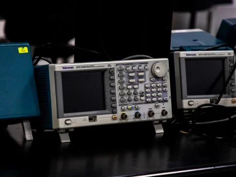
A semiconductor high-purity water plant uses three stages—makeup, primary purification, and polishing—to remove contaminants in sequence. Each stage has defined exit specs so downstream membranes and resins see only water they can polish without rapid fouling or resin exhaustion.
Stage 1: Makeup (Pretreatment)
Makeup pretreatment removes bulk solids, chlorine, and hardness from municipal or well water before RO. Exit targets are SDI below 3, turbidity below 0.1 NTU, and free chlorine below 0.1 ppm. Multimedia filters, activated carbon, softeners, and microfiltration do most of the work on variable raw water.
Efficient pretreatment with pretreatment systems for semiconductor UPW plants extends membrane and resin life on the primary train. Most plants we size for municipal feeds run at the lower end of chlorine and hardness loading after carbon and softener, which keeps RO cleaning intervals closer to 3–6 months than monthly shock cleans.
Stage 2: Primary Purification
Primary purification cuts dissolved solids, organics, and residual particles. Feed typically sits at SDI below 1 with very low turbidity. Exit targets are resistivity above 1 MΩ·cm, TOC below 50 ppb, and silica below 10 ppb before polish.
A 2-pass RO train delivering 98–99% salt rejection is the core step, followed by EDI or mixed-bed ion exchange and UV oxidation at 185/254 nm for early TOC cut. 2-pass RO systems for semiconductor UPW plants set the purity floor for polishing and protect CDI electrodes from hardness and silica spikes.
Stage 3: Polishing
Polishing finishes water for advanced nodes: resistivity above 18.2 MΩ·cm, TOC below 1 ppb, silica below 0.5 ppb, and particles below 100/mL at 0.05–0.1 μm. Ultrafiltration near 0.001 μm, membrane degasification targeting CO₂ below 1 ppb, and final mixed bed or Continuous Deionization (CDI) remove the last ions and particles.
Train selection follows the fab’s most sensitive tools. Critical RO trains, UV lamps, and high-pressure pumps usually run with 2N or N+1 redundancy. Automatic failover keeps UPW flowing when a primary unit trips, which limits downtime risk on continuous fabs that cannot idle CMP or wet benches.
Hydraulic design should state design flow, peak flow, and reclaim return separately. A 2,000 m³/day nameplate that ignores reclaim spikes will undersize polish during high rinse demand. Most plants we size for 300mm advanced nodes run average demand near the lower end of the day and peak 20–30% higher during wet-bench clusters.
Instrument taps belong on each stage exit, not only at the UPW tank. Stage-gate alarms on SDI, chlorine, RO permeate conductivity, TOC, and resistivity let operators isolate a failing skid before the loop inventory is contaminated. That practice turns the three-stage table from a drawing note into an operating procedure.
| Stage | Purpose | Key Technologies | Output Specifications |
|---|---|---|---|
| 1. Makeup (Pretreatment) | Remove bulk contaminants, protect downstream equipment. | Multimedia filters, Activated Carbon, Softeners, Microfiltration (MF) | SDI <3, Turbidity <0.1 NTU, Chlorine <0.1 ppm |
| 2. Primary Purification | Reduce TOC, ions, and particles significantly. | 2-pass Reverse Osmosis (RO), Electrodeionization (EDI), UV Oxidation (185/254 nm), Mixed Bed Ion Exchange (MBIX) | Resistivity >1 MΩ·cm, TOC <50 ppb, Silica <10 ppb |
| 3. Polishing | Achieve final ultra-high purity for advanced nodes. | Ultrafiltration (UF), Membrane Degasification, Final Mixed Bed Ion Exchange, Continuous Deionization (CDI) | Resistivity >18.2 MΩ·cm, TOC <1 ppb, Silica <0.5 ppb, Particles <100/mL (0.05-0.1 μm) |
TOC Reduction Technologies: UV vs. CDI vs. Mixed Bed Ion Exchange
TOC control to sub-1 ppb in semiconductor UPW usually compares UV oxidation, Continuous Deionization (CDI), and mixed bed ion exchange on influent quality, energy, and regeneration burden. Most plants we size for 3nm/5nm work run UV or hybrid UV+CDI at the lower end of influent TOC, typically below 50 ppb into polish.
UV Oxidation (185/254 nm)
Dual-wavelength UV (185 nm and 254 nm) oxidizes organics to CO₂ and H₂O and can hold TOC below 1 ppb when feed is already low. Energy use is typically 0.5–1 kWh/m³ treated. Lamp replacement for a medium system often runs $5,000–$10,000 per year, so lamp hours belong on the OPEX tracker beside power.
UV fits best when influent TOC is already below about 50 ppb. Pushing high-TOC RO permeate into UV alone burns energy and still leaves organic fragments that later raise resistivity noise in the loop.
Continuous Deionization (CDI)
CDI (electrodeionization) combines resins, selective membranes, and an electric field to remove ions and some organics without chemical regeneration. TOC below 2 ppb and recovery above 90% are common on well-pretreated feeds. CapEx for a 100 m³/h skid often sits at $300,000–$800,000.
CDI handles variable TOC loads better than batch mixed beds, but electrode fouling rises when pretreatment is weak. Keep hardness, free chlorine, and silica inside vendor limits or expect voltage creep and early module replacement.
Mixed Bed Ion Exchange
Mixed beds still deliver TOC below 1 ppb and very low ionic residuals on stable feeds. Regeneration with NaOH and HCl forces downtime and chemical waste. Chemical and waste OPEX typically runs $0.50–$1.00/m³ when regen frequency and haul costs are included.
Stable, low-TOC feeds suit mixed beds when chemical handling is already in place and the fab can tolerate scheduled regen windows. Variable tool-load organics usually push teams toward UV or hybrid polish instead.
Hybrid Systems
Hybrid UV plus CDI trains can hold TOC well below 1 ppb and cut energy by up to 30% versus a high-power UV-only polish. Confidential fab data from a 2025 TSMC facility indicated that hybrid polish supported 3nm production with more stable TOC and lower energy than UV alone. That pattern matches what we see when polish influent sits near 20–40 ppb TOC rather than near the 50 ppb ceiling.
| Technology | Achievable TOC | Key Advantages | Key Disadvantages | Typical OPEX |
|---|---|---|---|---|
| UV Oxidation (185/254 nm) | <1 ppb | No chemicals, highly effective for low TOC. | High energy consumption, frequent lamp replacement. | $0.50–$1.00/m³ (energy, lamps) |
| Continuous Deionization (CDI) | <2 ppb | No chemical regeneration, high water recovery, stable. | Higher CapEx, potential electrode fouling. | $0.30–$0.60/m³ (energy, maintenance) |
| Mixed Bed Ion Exchange | <1 ppb | Excellent final polishing for ions and TOC. | Requires chemical regeneration, downtime, chemical waste. | $0.50–$1.00/m³ (chemicals, waste) |
What Is the Water Treatment Plant Cost Breakdown?
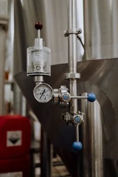
A 2,000 m³/day semiconductor UPW plant typically needs $2.5M–$3.5M CapEx, while broader 1,000–3,000 m³/day packages fall in the $1.2M–$4.5M band. Engineers and procurement teams use these splits to compare bids, set contingency, and separate UPW polish from solvent reclaim budgets.
Capital Expenditure (CapEx) Breakdown
For a new 2,000 m³/day plant built to 3nm/5nm UPW specs, CapEx commonly lands between $2.5M and $3.5M. Primary purification dominates because 2-pass RO, EDI, and primary UV carry the salt and TOC load:
- Pretreatment: 20% ($500K–$700K) for multimedia filters, activated carbon, and softeners.
- Primary Purification: 50% ($1.25M–$1.75M) for 2-pass RO, EDI, and primary UV.
- Polishing: 20% ($500K–$700K) for UF, degasification, and final mixed beds or CDI.
- Monitoring & Controls: 10% ($250K–$350K) for online analyzers, PLCs, and SCADA.
Operational Expenditure (OPEX) Breakdown
Producing semiconductor UPW typically costs $0.80–$1.50/m³, driven by local power, chemicals, and labor. Energy is usually the largest single line when UV polish and high-pressure RO run continuously:
- Energy: 30–40% ($0.25–$0.60/m³) for pumps, UV, and EDI/CDI.
- Chemicals: 20–30% ($0.15–$0.45/m³) for antiscalants, biocides, cleaners, and NaOH/HCl regeneration. Tight chemical dosing for UPW resin regeneration keeps this band in check.
- Membrane/Resin Replacement: 20–30% ($0.15–$0.45/m³) for RO, UF, and ion-exchange media.
- Labor & Maintenance: 10% ($0.08–$0.15/m³) for operations and preventive work.
What Does an IPA Level 0 Cost Breakdown Include?
An IPA Level 0 cost breakdown sits outside the UPW CapEx table above. Isopropyl alcohol reclaim and Level 0 solvent loops are budgeted as solvent-recovery CapEx/OPEX, not as a share of the $2.5M–$3.5M UPW plant. When finance teams ask for an IPA Level 0 cost breakdown beside UPW figures, keep solvent recovery, drum handling, and analytical QC separate. Do not mix those costs into the $0.80–$1.50/m³ UPW OPEX.
Procurement packages that blend IPA reclaim into UPW line items make bid comparison harder. Hold two work breakdown structures: one for UPW makeup through polish, one for IPA Level 0 reclaim and waste solvent handling.
Cost drivers that move a 2,000 m³/day plant inside the $2.5M–$3.5M CapEx band include raw-water TDS, required redundancy (2N versus N+1), online metals/TOC analyzer count, and civil/electrical scope. Softener and carbon sizing track hardness and chlorine; RO and EDI sizing track TDS and silica; polish sizing tracks particle and TOC targets for the node.
OPEX sensitivity is dominated by power tariff and membrane life. At $0.25–$0.60/m³ energy inside a $0.80–$1.50/m³ total, a high tariff site should favor lower-pressure RO and hybrid TOC polish over UV-heavy designs. Chemical costs of $0.15–$0.45/m³ rise when regen frequency climbs, so resin capacity and RO rejection remain linked line items.
Return on Investment (ROI) Calculation
A 1% yield gain in a 5nm fab can save more than $1 million per month. Payback on a UPW upgrade commonly falls in 12–18 months when scrap reduction is measured against wafer ASP. A $3 million plant that enables a 2% yield gain ($2 million/month) would pay back in about 1.5 months under that yield model.
Detailed ROI sheets should use the fab’s own wafer ASP, scrap rates, and ramp utilization. Template calculators help, but the yield delta must come from metrology tied to UPW excursions, not a generic marketing factor.
Hidden Costs
Budget items that often sit outside the base quote include redundancy hardware, third-party compliance testing, and emergency response retainers:
- Redundancy: 2N or N+1 on critical skids can add 20–30% CapEx.
- Compliance Testing: Third-party certification often costs $50K–$100K per year.
- Emergency Response Plans: UPW failure plans typically add $20K–$50K per year to maintain.
| Cost Category | Breakdown for 2,000 m³/day Plant | Details |
|---|---|---|
| CapEx (Total) | $2.5M – $3.5M | Initial investment for equipment and installation. |
| Pretreatment | 20% ($500K – $700K) | Multimedia filters, activated carbon, softeners. |
| Primary Purification | 50% ($1.25M – $1.75M) | RO, EDI, primary UV. |
| Polishing | 20% ($500K – $700K) | UF, degasification, final MB/CDI. |
| Monitoring & Controls | 10% ($250K – $350K) | Sensors, PLCs, SCADA. |
| OPEX (per m³) | $0.80 – $1.50/m³ | Ongoing operational costs. |
| Energy | 30-40% ($0.25 – $0.60/m³) | Power for pumps, UV, EDI. |
| Chemicals | 20-30% ($0.15 – $0.45/m³) | Antiscalants, biocides, regeneration chemicals. |
| Membrane/Resin | 20-30% ($0.15 – $0.45/m³) | Replacement costs for consumables. |
| Labor & Maintenance | 10% ($0.08 – $0.15/m³) | Operational staff and routine servicing. |
| ROI Payback Period | 12 – 18 months | Based on yield improvement savings. |
Equipment Selection: 5 Critical Criteria for Semiconductor UPW Plants
Stable UPW supply depends on five equipment criteria: redundancy, online monitoring, material compatibility, supplier semiconductor track record, and modular expansion paths. Skipping any one of these shows up later as downtime, leachate excursions, or forced retrofit during a node transition.
- Redundancy: Critical high-pressure pumps, RO trains, UV lamps, and primary sensors need 2N or N+1. Documented failover tests confirm backup units take load without UPW interruption during peak tool demand.
- Real-time Monitoring: Online TOC analyzers with <1 ppb accuracy, particle counters for 0.05–0.1 μm, and resistivity sensors that hold above 18.2 MΩ·cm are baseline. Instruments should follow SEMI F47 calibration practice and raise alerts on drift before wafers see the excursion.
- Material Compatibility: PVDF or PFA piping limits extractables into the circulating loop. Passivated stainless steel 316L suits tanks and valves. PVC and copper are avoided because they leach ions and organics into UPW during heat and stagnation.
- Supplier Track Record: Prefer vendors with at least 5 years on semiconductor UPW, ideally with 3nm/5nm references. Ask for ISO 14644-1 cleanroom manufacturing evidence and detailed case data on high-purity delivery and service response times.
- Future-proofing: Modular skids should allow growth from 2,000 to 3,000 m³/day without a full rebuild. Leave headroom for tighter PFAS or emerging-contaminant limits expected in 2027 reviews so civil and header work is not repeated.
How Does Variable Chemistry Affect Semiconductor Wastewater Design?
Variable chemistry in semiconductor wastewater design comes from shifting etch, CMP, and clean chemistries that change pH, fluoride, copper, and oxidant loads shift to shift. UPW makeup volume and reclaim rate set the hydraulic load, but the wastewater train must track recipe changes that UPW polish never sees.
Most plants we support keep UPW and wastewater on separate PFDs with shared utilities only at the battery limit. When municipal or industrial cost models are needed for comparison, a regional reference such as chlie wastewater treatment process cost helps frame CapEx/OPEX language—not UPW polish specs.
Compact fab drains and utility buildings often use an Underground Package Sewage Treatment Plant (WSZ Series) for sanitary and low-strength streams while fluoride and metals stay on dedicated treatment. That split keeps sanitary BOD from diluting metals precipitation and keeps UPW regenerate brine on a controlled path.
Selection checklist for variable-chemistry fabs:
- Map each tool drain to equalize, neutralize, or metals precipitation before biological steps.
- Size equalization for the worst 24-hour recipe swing, not the monthly average flow.
- Keep fluoride and copper trains isolatable when tool mixes change during ramp.
- Confirm UPW reject and regenerate waste have dedicated paths into the wastewater balance.
- Hold spare chemical dosing capacity of at least 20–30% for recipe ramps.
- Require online pH, ORP, and conductivity at each major junction box.
- Revisit sludge and brine haul costs whenever reclaim rate or IPA reclaim volume rises.
Case Study: How a 5nm Fab Reduced Yield Losses by 18% with a UPW Upgrade
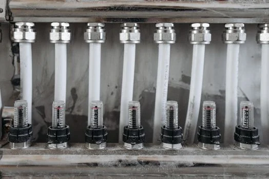
A 5nm fab in Taiwan cut yield losses by 18% after a targeted UPW upgrade. Before the project, yield loss sat at 8% while resistivity held near 17.8 MΩ·cm, below the ASTM E-1.3 2026 target above 18.2 MΩ·cm.
Particle and ionic wafer defects traced to the UPW loop after metrology ruled out tool recipe drift. The existing plant met older nodes but could not hold 5nm polish limits on TOC and particles. HydropureWater worked with the fab on a three-stage upgrade scoped to the 2,500 m³/day demand.
The design added CDI for TOC control and 0.001 μm ultrafiltration for final particle polish. CapEx for the 2,500 m³/day upgrade was $3.2 million, inside the broader $1.2M–$4.5M band used for 1,000–3,000 m³/day plants.
After commissioning, resistivity held above 18.2 MΩ·cm, TOC fell below 1 ppb, and silica fell below 0.5 ppb. Yield loss moved from 8% to 6.56%—an 18% relative reduction—saving about $1.8 million per month in scrap and paying back the $3.2 million outlay in 14 months.
Online TOC and particle monitors mattered as much as the skids. A rising TOC trend flagged a failing UV lamp within 2 hours. Lamp replacement avoided a projected 3% yield loss that would have landed if the fault ran another shift. That event is why SEMI F47-aligned analyzers belong in CapEx, not as a deferred option.
UPW Design Decision Checklist
Before freezing a UPW P&ID, walk this checklist with process, facilities, and yield engineering in the same meeting. Gaps here show up later as change orders or wafer holds.
- Confirm node target (5nm, 3nm, or 2nm roadmap) and whether SEMI F63 2025 <5nm limits apply.
- Lock polish exit specs: resistivity >18.2 MΩ·cm, TOC <1 μg/L (or <0.5 μg/L), silica <0.5 ppb (or <0.2 ppb).
- State design and peak flow in m³/day, plus reclaim return assumptions.
- Choose redundancy class (N+1 or 2N) for RO, UV, and high-pressure pumps.
- Select TOC polish path: UV, CDI, mixed bed, or hybrid, with OPEX bands assigned.
- Specify piping materials (PVDF/PFA) and ban PVC/copper on UPW wetted paths.
- Budget online TOC, particles, and resistivity under SEMI F47 calibration practice.
- Separate IPA Level 0 reclaim CapEx/OPEX from the UPW $2.5M–$3.5M (2,000 m³/day) model.
- Align wastewater equalization with variable chemistry drains and UPW regenerate brine.
- Set payback logic on measured yield delta, using the 12–18 month band as a planning check.
Use the checklist as the agenda for vendor bid reviews. Every exception should carry a named risk owner and a temporary operating limit, not a silent datasheet footnote.
Who This Is For and Next Step
This guide is for fab facilities engineers, EPC process leads, and procurement managers sizing or upgrading UPW for 3nm/5nm work. Teams that only need municipal or food-grade water should look at simpler RO packages instead of full UPW polish trains.
If you are comparing stage splits, redundancy, or a CapEx band against your flowsheet, send your raw-water analysis and target node specs through our UPW plant inquiry form for a scoped equipment list.
Frequently Asked Questions
What is the difference between ultrapure water (UPW) and high-purity water?
Ultrapure water for semiconductors follows limits such as ASTM E-1.3 resistivity above 18.2 MΩ·cm, TOC below 1 μg/L, and silica below 0.5 ppb. High-purity water is a broader label used in pharma or power plants under USP, EP, or boiler chemistry rules. Those grades do not require the same sub-nanometer particle and trace-ion control that advanced-node UPW demands at the point of use.
How often should UPW plant membranes be replaced?
RO membranes typically last 3–5 years, EDI modules 5–7 years, and UF membranes 3–5 years under normal semiconductor UPW duty. Replace earlier when differential pressure rises more than 15%, permeate quality stays off-spec after cleaning, or flux falls and cannot be recovered by CIP. Cleaning history, free chlorine events, and silt loading shorten those ranges on hard or high-SDI raw water.
What are the most common causes of UPW contamination?
Colloidal silica, organics, and bacteria cause most UPW excursions. Silica often follows weak RO rejection or membrane shedding. Organics leach from resins, grow in biofilms, or pass incomplete TOC oxidation. Bacteria colonize dead legs and tanks. Strong pretreatment, scheduled cleans, loop sanitization, and continuous flow design limit those sources.
Can a UPW plant be upgraded for 2nm nodes?
Yes. Upgrades for 2nm usually add polish stages, deeper degasification, and ultra-low boron resins targeting below 0.05 ppb, plus tighter online trace monitoring. CapEx often lands at 20–30% of the original plant cost, depending on how close the current train already sits to sub-5nm SEMI F63 limits.
How does UPW quality affect EUV lithography?
EUV lithography at 13.5 nm needs UPW free of particles near 10 nm during develop and clean steps. Particles that size can bridge fine features and create shorts on 3nm/2nm patterns. EUV-ready UPW therefore tightens particle counts, dissolved gases, and trace metals beyond older deep-UV rinse limits used on prior nodes.