Semiconductor Wastewater Reuse: Engineering Specs, 85%+ Recovery Rates & Cost-Optimized Equipment Guide 2025
Semiconductor fabs can achieve wastewater reuse rates up to 85% for 8-inch wafer production and 60-70% for 12-inch wafers, with recovery rates exceeding 90% in optimized systems. Key contaminants—including total suspended solids (TSS) at 500-2000 mg/L, chemical oxygen demand (COD) at 300-1500 mg/L, heavy metals like Cu, Ni, and Zn at 1-10 mg/L, and silica at 50-200 mg/L—require multi-stage treatment. Effective systems utilize ZSQ series DAF systems for semiconductor wastewater pretreatment for solids removal, MBR or RO for organics and ions, and polishing with ion exchange or EDI for UPW-grade reuse. Costs range from $0.50 to $2.50 per cubic meter treated, with payback periods of 2-5 years depending on local water pricing and system scale.
For a facility manager in an arid semiconductor hub like Arizona or Tainan, the technical challenge is no longer just compliance; it is operational survival. When municipal water costs climb toward $10/m³ and discharge limits for total dissolved solids (TDS) become more restrictive, the engineering focus shifts from simple treatment to high-efficiency reclamation. This guide provides the technical specifications and financial frameworks necessary to design and implement these high-recovery systems.
Why Semiconductor Fabs Must Prioritize Wastewater Reuse in 2025
Global water scarcity projections indicate that 20% of the world’s population will lack access to potable water by 2050, creating a direct risk to water-intensive industries like semiconductor manufacturing. A single 12-inch wafer requires approximately 10 cubic meters of water during its fabrication cycle, leading modern "mega-fabs" to consume between 2 million and 10 million gallons of water per day. This high water intensity makes the industry a primary target for both regulatory scrutiny and resource-related production bottlenecks.
Regulatory pressures are accelerating the adoption of reuse technologies. For instance, Taiwan’s 2024 water reuse mandates require large industrial users to achieve specific reclaimed water targets, with a hypothetical compliance timeline requiring 50% reuse by 2026 for new facilities. Failure to meet these mandates can result in significant fines or, more critically, the denial of expansion permits in water-stressed regions.
The economic drivers for reuse are equally compelling. In arid regions, water pricing often ranges from $5 to $15 per cubic meter, whereas water-rich areas may charge only $0.50 to $2 per cubic meter. For a fab processing 50,000 m³ per day, a 70% reuse rate can save over $100 million in cumulative operating costs over a five-year period. These savings are calculated by subtracting the OPEX of the reuse system ($0.50–$2.50/m³) from the cost of raw water purchase and the avoided costs of wastewater discharge fees and chemical surcharges.
Contaminant Profile of Semiconductor Wastewater: What Must Be Removed for Reuse
Semiconductor effluent is a complex mixture of inorganic acids, organic solvents, and abrasive slurries used in Chemical Mechanical Planarization (CMP). According to EPA 2023 semiconductor effluent guidelines, typical influent characteristics include a volatile pH range of 2-12, TSS levels between 500 and 2000 mg/L, and COD concentrations from 300 to 1500 mg/L. These parameters vary significantly between the "front-end-of-line" (FEOL) cleaning and "back-end-of-line" (BEOL) packaging processes.
Heavy metals such as Copper (1-10 mg/L), Nickel (0.5-5 mg/L), and Zinc (2-20 mg/L) originate primarily from etching and plating stages. These must be reduced to sub-ppb levels if the water is destined for Ultrapure Water (UPW) makeup. silica (50-200 mg/L) and fluoride (10-100 mg/L) from wafer cleaning pose severe scaling risks for Reverse Osmosis (RO) membranes, requiring specific chemical precipitation or specialized DAF pretreatment to prevent membrane fouling.
Organic solvents like Isopropyl Alcohol (IPA), acetone, and Various glycols (10-100 mg/L) contribute to the COD load. While these are biodegradable, their high volatility requires robust biological treatment or advanced oxidation processes (AOP). To reach UPW compatibility per the SEMI F63-0705 standard, the final effluent must achieve Total Organic Carbon (TOC) levels of < 1 µg/L and a resistivity of > 18 MΩ·cm.
| Contaminant | Influent Range (mg/L) | Target for Reuse (mg/L) | Primary Treatment Technology |
|---|---|---|---|
| TSS (CMP Slurry) | 500 - 2,000 | < 5 | DAF + Multi-Media Filtration |
| COD (Solvents) | 300 - 1,500 | < 20 | MBR (Membrane Bioreactor) |
| Heavy Metals (Cu, Ni) | 1 - 10 | < 0.05 | Chemical Precipitation + DAF |
| Silica (SiO₂) | 50 - 200 | < 1 | Activated Alumina or Softening |
| Fluoride (F⁻) | 10 - 100 | < 1 | Calcium Chloride Precipitation |
Treatment Process Flow for 85%+ Wastewater Reuse: Engineering Specs and Recovery Rates
Achieving recovery rates above 85% requires a multi-stage, integrated treatment train that addresses both particulate and dissolved contaminants. The process begins with pretreatment using rotary mechanical bar screens (GX Series), which provide 95% efficiency in removing coarse solids at 3 mm spacing, protecting downstream pumps and membranes from mechanical damage.
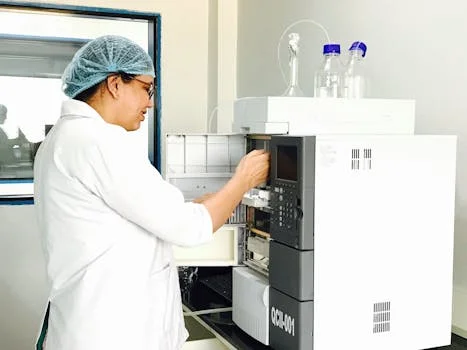
Primary treatment utilizes ZSQ series DAF systems for semiconductor wastewater pretreatment. These systems achieve 92-97% TSS reduction by injecting micro-bubbles (20-40 microns) that attach to flocculated particles, floating them to the surface for skimming. For semiconductor wastewater, DAF is superior to traditional sedimentation because it effectively handles the low-density particles found in CMP slurries. Following DAF, integrated MBR systems for COD and BOD removal in semiconductor fabs are employed. These systems combine biological degradation with ultrafiltration, typically achieving 85-95% COD reduction with a Hydraulic Retention Time (HRT) of 6-10 hours and a Sludge Retention Time (SRT) of 15-30 days.
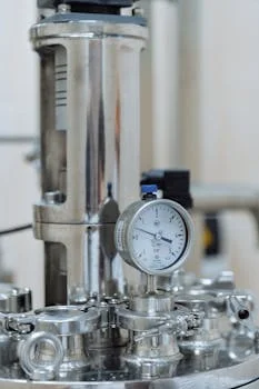
Tertiary treatment is the core of the reuse engine. High-recovery RO systems for semiconductor wastewater reuse utilize thin-film composite membranes with pore sizes around 0.0001 microns. These systems are designed for 95% recovery and 99.5% ion rejection. To maintain these rates, PLC-controlled chemical dosing for semiconductor wastewater treatment is essential for scale inhibition and pH adjustment. For UPW-grade reuse, Electrodeionization (EDI) provides final polishing, removing trace ions to reach 18 MΩ·cm resistivity.
| Treatment Stage | Equipment Type | Key Engineering Spec | Removal Efficiency |
|---|---|---|---|
| Pretreatment | DAF (ZSQ Series) | Air-to-Solids Ratio: 0.02 - 0.05 | 95% TSS, 90% FOG |
| Biological | MBR (Integrated) | Flux: 15 - 25 LMH | 90% COD, 99% Turbidity |
| Demineralization | RO (High Recovery) | Operating Pressure: 150 - 400 psi | 99.5% Salt Rejection |
| Disinfection | ClO₂ Generator | Dosage: 0.5 - 2.0 mg/L | 99.9% Microbial Kill |
| Sludge Handling | Filter Press | 30-40% Dry Solids Content | 98% Solids Capture |
Recovery Rate Benchmarks: How Different System Configurations Compare
The selection of a system configuration depends on the intended reuse application and the capital budget. Basic reuse, such as cooling tower makeup or landscaping, typically targets a 60% recovery rate. This is achieved through DAF and sand/carbon filtration, removing the bulk of TSS and organic matter but leaving high TDS levels that would be corrosive to process equipment.
Moderate reuse applications, including scrubber water and Clean-in-Place (CIP) rinse cycles, require 75% recovery. This configuration adds an MBR stage to the DAF pretreatment, ensuring that organic loads do not foul the subsequent RO membranes. For high-purity reuse, where reclaimed water is fed back into the UPW system, an 85-90% recovery rate is required. This necessitates a "double-pass" RO system followed by EDI polishing. Discover how MBR systems work for semiconductor wastewater treatment in these high-recovery contexts to see how they protect RO membranes from biofouling.
Zero Liquid Discharge (ZLD) represents the technical ceiling, achieving 95%+ recovery. ZLD systems utilize thermal evaporators and crystallizers to convert the RO brine into solid waste and high-purity distillate. While ZLD eliminates discharge fees, it is the most energy-intensive option, with costs per cubic meter often triple that of standard RO systems. A case study of an 8-inch wafer fab in East Asia demonstrated that by combining DAF, MBR, and a three-stage RO array, they achieved a stable 85% reuse rate, significantly reducing their reliance on local groundwater.
| Reuse Tier | Recovery Rate | Typical Configuration | Application |
|---|---|---|---|
| Basic | 50 - 60% | DAF + Filtration | Cooling Towers, Landscaping |
| Moderate | 70 - 75% | DAF + MBR + RO (Single Pass) | Scrubbers, General Rinsing |
| High-Purity | 85 - 90% | DAF + MBR + RO (Double Pass) + EDI | UPW Makeup, Process Water |
| ZLD | 95% + | RO + Evaporator + Crystallizer | Total Water Independence |
Cost-Benefit Analysis: CAPEX, OPEX, and Payback Periods for Reuse Systems
The financial viability of a semiconductor wastewater reuse system is determined by the intersection of Capital Expenditure (CAPEX) and Operating Expenditure (OPEX) against the cost of municipal water. CAPEX for these systems typically ranges from $500 to $2000 per m³/day of capacity. The primary cost drivers include the degree of automation (PLC/SCADA integration), the quality of membrane materials, and the complexity of the pretreatment train needed for specific contaminants like silica.
OPEX usually falls between $0.50 and $2.50 per cubic meter of treated water. This includes energy consumption (0.8–1.5 kWh/m³ for RO-based systems), chemical consumables (antiscalants, coagulants), membrane replacement cycles (typically every 3-5 years), and labor. Learn how industrial RO systems achieve 99.5% contaminant removal while optimizing energy use through energy recovery devices (ERDs).
Payback periods vary drastically by geography. In Arizona, where water costs can reach $10/m³, a 10,000 m³/day reuse system can pay for itself in under 2 years. In regions like Taiwan, with lower baseline water costs ($2/m³), the payback may extend to 4-5 years, but the ROI is often bolstered by avoided discharge fees and regulatory incentives. For example, a 12-inch fab in Singapore recently reduced its total water procurement costs by 40% after implementing a 70% reuse system, achieving a full return on investment in just 3.2 years.
| Cost Component | Estimated Value | Impact on ROI |
|---|---|---|
| CAPEX | $500 - $2,000 per m³/day | Initial investment; sensitive to scale |
| OPEX (Energy) | $0.20 - $0.60 per m³ | Ongoing; can be reduced with ERDs |
| OPEX (Chemicals) | $0.15 - $0.40 per m³ | Dependent on influent chemistry |
| Membrane Replacement | $0.10 - $0.30 per m³ | Predictable maintenance cost |
| Payback Period | 2 - 5 Years | Highly dependent on local water rates |
Selecting the Right Equipment: Decision Framework for Semiconductor Fabs
Selecting a wastewater reuse system requires a structured engineering evaluation to ensure the treatment train matches the specific effluent profile and reuse goals of the fab. The following five-step framework is recommended for procurement and EHS teams:
- Step 1: Define Reuse Application: Determine if the water is for low-grade use (cooling towers) or high-grade use (UPW makeup). This dictates whether you need a simple DAF-filtration setup or a full MBR-RO-EDI train.
- Step 2: Characterize Wastewater: Conduct comprehensive sampling across different shifts and process cycles. Pay close attention to silica, fluoride, and TOC fluctuations, as these dictate the pretreatment requirements.
- Step 3: Evaluate Scalability: Semiconductor fabs often expand in phases. Modular treatment systems (like skid-mounted MBR or RO units) allow for incremental capacity increases without over-investing in CAPEX during the initial phase.
- Step 4: Assess Automation: Modern fabs require high-level integration. Ensure the equipment supports PLC/SCADA protocols for remote monitoring and automated PLC-controlled chemical dosing for semiconductor wastewater treatment.
- Step 5: Compare Vendor Proposals: Use a weighted scoring matrix that includes not just initial price, but guaranteed recovery rates, energy consumption per m³, and local technical support availability.
For more detailed engineering insights, you can learn how industrial RO systems achieve 99.5% contaminant removal and how to integrate them into a broader fab water management strategy.
Frequently Asked Questions
What is the maximum recovery rate achievable for 12-inch wafer fabs?
While 8-inch fabs can reach 85%, 12-inch fabs typically achieve 60-70% reuse due to the higher purity requirements of the more advanced nodes. However, with ZLD technologies, these rates can exceed 90% at the cost of higher energy consumption.
How does silica affect RO membrane lifespan in semiconductor reuse?
Silica is a major scaling agent. If levels exceed 50 mg/L in the RO feed, it can precipitate and cause irreversible membrane fouling. Pretreatment with activated alumina or specialized chemical precipitation in a DAF unit is required to keep silica levels below 1 mg/L for the RO stage.
What is the average OPEX for an MBR-RO reuse system?
The average OPEX is between $1.20 and $1.80 per cubic meter. This includes electricity for high-pressure RO pumps, membrane aeration in the MBR, and chemical consumables for pH adjustment and cleaning-in-place (CIP).
Can reclaimed wastewater be used for UPW makeup?
Yes, provided the treatment train includes MBR, double-pass RO, and EDI polishing. The final water must meet SEMI F63 standards, with TOC < 1 ppb and resistivity > 18 MΩ·cm, to ensure it does not impact wafer yield.