Semiconductor Wastewater Treatment Projects: Engineering Specs, Cost Data & Zero-Liquid Discharge Design Guide 2025
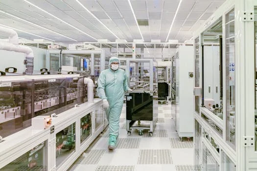
Semiconductor wastewater treatment projects require specialized engineering to handle high concentrations of fluoride (up to 1,000 mg/L), ammonia (50–300 mg/L), and metals (e.g., copper, nickel) while meeting stringent discharge limits or enabling water reuse. A $417M project by a leading semiconductor manufacturer demonstrated 95% water recovery using Biological Nutrient Removal (BNR) and Membrane Bioreactor (MBR) technology, reducing potable water purchases by 30% (MWH Constructors, 2026). Key challenges include chelate degradation (addressed via advanced oxidation) and hydrofluoric acid neutralization (requiring pH adjustment and precipitation). Modular, skid-mounted systems can accelerate deployment by 40% compared to conventional builds (SAMCO Technologies, 2023).Why Semiconductor Fabs Need Custom Wastewater Treatment Projects
Semiconductor manufacturing processes, including chemical mechanical polishing (CMP), etching, and rinsing, generate diverse wastewater streams containing high concentrations of fluoride (typically 500–1,000 mg/L), ammonia (50–300 mg/L), and metals like copper (10–50 mg/L), alongside persistent chelating agents such as EDTA. These complex contaminant profiles necessitate custom-engineered wastewater treatment projects to ensure compliance with increasingly stringent environmental regulations. Publicly Owned Treatment Works (POTW) standards often require discharge limits as low as <10 mg/L for fluoride, <1 mg/L for copper, and <5 mg/L for Total Suspended Solids (TSS), as outlined by EPA 40 CFR Part 469 and local ordinances. Beyond regulatory compliance, severe water scarcity in regions with high semiconductor manufacturing density drives the imperative for water reuse. A typical 300mm fabrication facility consumes between 2 and 4 million gallons of water per day; implementing advanced water reuse projects can reduce potable water purchases by 30–50% (MWH Constructors, 2026). global regulatory trends, such as China’s GB 31573-2015 and Taiwan’s EPA standards, are continually tightening limits on fluoride and heavy metals, increasing the financial and operational burden of non-compliance.Contaminant Profile: What’s in Semiconductor Wastewater and Why It’s Hard to Treat
| Contaminant | Primary Source | Typical Concentration | Key Treatment Challenge | Removal Efficiency (Typical) |
|---|---|---|---|---|
| Fluoride (F⁻) | HF etching | 50–1,000 mg/L | Precise pH control (8.5–9.5) for CaF₂ precipitation; sludge handling | >99% (precipitation) |
| Ammonia (NH₃/NH₄⁺) | NH₄OH cleaning | 50–300 mg/L | Long SRTs for biological nitrification/denitrification | 90–95% (biological) |
| Metals (Cu, Ni, As) | CMP, plating, GaAs wafers | 10–50 mg/L | Chelate binding, requiring pre-treatment or AOP | 95–99% (precipitation, ion exchange) |
| Chelating Agents (EDTA) | CMP, cleaning solutions | 5–50 mg/L TOC equivalent | Inhibit metal precipitation; require strong oxidants | >90% (AOP) |
| Organics (TOC) | Photoresists, solvents | 50–500 mg/L | Biodegradability, removal to trace levels for reuse | 95% (MBR), <1 mg/L (RO polishing) |
Treatment Technology Comparison: MBR vs. Advanced Oxidation vs. RO for Semiconductor Wastewater
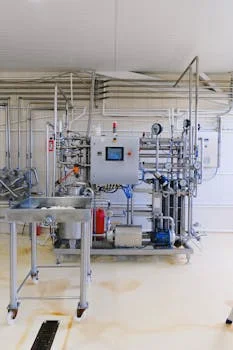
Effective semiconductor wastewater treatment often relies on a combination of advanced physical, chemical, and biological technologies, each optimized for specific contaminant removal and water quality targets. The Membrane Bioreactor (MBR) system, which combines activated sludge biological treatment with ultrafiltration membranes (typically 0.1 μm pore size), is ideal for high-efficiency removal of Total Suspended Solids (TSS), Chemical Oxygen Demand (COD), and ammonia. A notable project achieved 95% water recovery using MBR technology (MWH Constructors, 2026). However, MBR systems have limitations, including relatively high energy consumption (0.8–1.2 kWh/m³) and susceptibility to membrane fouling, particularly from silica in semiconductor wastewater. Explore our MBR systems for semiconductor wastewater reuse. Advanced Oxidation Processes (AOPs), such as UV/H₂O₂ or O₃/H₂O₂, are critical for the destruction of persistent organic compounds and chelating agents that resist conventional biological treatment. AOPs can achieve over 90% TOC removal, typically within 30–60 minutes of reaction time. The primary drawbacks of AOPs include high chemical costs, ranging from $0.50–$1.50/m³ for hydrogen peroxide or ozone generation, and the potential need for residual H₂O₂ quenching before subsequent treatment stages. Discover how electrocoagulation can remove metals and chelates from semiconductor wastewater, or learn how ClO₂ generators can disinfect semiconductor wastewater for reuse. Reverse Osmosis (RO) systems are indispensable for removing dissolved ions, achieving 95–99% rejection rates, and producing ultrapure water suitable for various reuse applications within semiconductor fabs. A 600 GPM hydrofluoric acid wastewater treatment plant deployed RO to achieve high-quality effluent (Saltworks Technologies, 2025). Key limitations of RO include the generation of a concentrated brine stream, typically 20–30% of the feed volume, which requires specialized disposal, and the risk of membrane scaling from high concentrations of silica or calcium. Discover our RO systems for ultrapure water reuse in semiconductor fabs. Often, hybrid systems are employed to meet stringent water quality targets. For instance, an MBR system followed by RO can produce water suitable for cooling tower makeup or other non-potable uses, while an AOP combined with chemical precipitation can facilitate Zero Liquid Discharge (ZLD). A significant project demonstrated a hybrid approach, utilizing BNR/MBR, RO, and evaporation technologies to achieve 95% water recovery (MWH Constructors, 2026). The choice between modular, skid-mounted systems and conventional stick-built plants also influences project timelines and costs. Modular systems can reduce installation time by approximately 40% but typically have a higher CAPEX ($1,500–$2,500/m³ of capacity) compared to conventional builds ($1,000–$1,800/m³).| Technology | Primary Application | Key Contaminants Removed | Efficiency (Typical) | Advantages | Limitations | Typical Energy Use |
|---|---|---|---|---|---|---|
| Membrane Bioreactor (MBR) | Biological treatment, solids separation | TSS, COD, BOD, Ammonia | >95% TSS, >90% COD, 90–95% NH₄-N | High effluent quality, small footprint | High energy use, membrane fouling (silica) | 0.8–1.2 kWh/m³ |
| Advanced Oxidation Process (AOP) | Chelate & recalcitrant organic destruction | Chelates (EDTA), TOC, specific organics | >90% TOC removal | Effective for non-biodegradables, minimal sludge | High chemical cost, residual oxidant quenching | 0.5–1.5 kWh/m³ (indirect from chemical production) |
| Reverse Osmosis (RO) | Dissolved solids removal, water polishing | Ions, salts, trace organics, fluoride | 95–99% rejection of dissolved solids | Produces ultrapure water, high recovery | Brine disposal, scaling potential, pre-treatment required | 1.5–3.0 kWh/m³ |
| Chemical Precipitation | Metals, fluoride removal | Heavy metals (Cu, Ni), Fluoride (F⁻) | >99% for F⁻, >95% for metals | Cost-effective for bulk removal | Sludge generation, pH sensitivity | 0.1–0.3 kWh/m³ (for mixing, pumping) |
Zero Liquid Discharge (ZLD) vs. Water Reuse: Cost-Benefit Analysis and Decision Framework
| Feature | Zero Liquid Discharge (ZLD) Strategy | Water Reuse Strategy |
|---|---|---|
| Definition | 95–99% water recovery; solid waste disposal | 70–90% water recovery; non-potable applications |
| CAPEX Range (per m³ capacity) | $3.00–$5.00 | $1.50–$3.00 |
| OPEX Range (per m³) | $1.50–$3.50 | $0.50–$2.00 |
| Typical Water Recovery | 95–99% | 70–90% |
| Energy Footprint (kg CO₂/m³) | 0.5–1.0 | 0.2–0.5 |
| Key Drivers for Selection | Severe water scarcity, ultra-strict discharge, corporate water neutrality goals | Existing non-potable demand, CAPEX constraints, high energy costs |
Project Cost Breakdown: CAPEX, OPEX, and ROI for Semiconductor Wastewater Treatment
A comprehensive understanding of capital expenditure (CAPEX), operational expenditure (OPEX), and return on investment (ROI) is essential for successfully budgeting and justifying semiconductor wastewater treatment projects. CAPEX components typically include equipment (40–50% of the total project cost), civil works (20–30%), installation (15–20%), and engineering services (10–15%). For instance, a $417M project allocated approximately 45% of its budget to core equipment, including BNR/MBR, RO, and evaporation units (MWH Constructors, 2026). OPEX for semiconductor wastewater treatment plants is driven by several factors: energy consumption accounts for 30–40% of the total OPEX, chemicals for 20–30%, labor for 15–20%, and maintenance for 10–15%. A 600 GPM hydrofluoric acid wastewater treatment plant reported an OPEX of $0.80/m³, with energy costs representing $0.30/m³ of that total (Saltworks Technologies, 2025). Learn more about wastewater treatment plant costs and ROI calculations. The Return on Investment (ROI) for these projects is driven by tangible savings and avoided costs. Water savings, particularly for potable water, can range from $0.50–$2.00/m³, directly reducing operational expenses. Avoiding regulatory fines, which can range from $10,000–$100,000 per violation, provides significant financial protection. Additionally, sustainability incentives, such as tax credits for water reuse or carbon footprint reductions, can enhance ROI. A 1 MGD (million gallons per day) reuse project, with an OPEX of $1.50/m³ and water savings of $1.00/m³, can achieve payback within 3–5 years. Several strategies can optimize project costs. Modular design, incorporating prefabricated skid-mounted units, can reduce overall CAPEX by 10–20% by minimizing on-site construction time and labor. Energy recovery systems, such as those integrated with RO brine concentrators, can cut energy consumption by up to 30%. Implementing advanced automation and control systems, including PLC-based remote monitoring, can reduce labor costs by 20–30% and enable predictive maintenance, minimizing downtime.| Cost Category | Typical % of Total | Key Drivers | Example Data/Impact |
|---|---|---|---|
| CAPEX: Equipment | 40–50% | Technology choice (MBR, RO, AOP, ZLD), capacity, material of construction | $417M project allocated 45% to equipment (MWH Constructors, 2026) |
| CAPEX: Civil Works | 20–30% | Site preparation, foundation, building, tankage | Varies by site complexity and footprint |
| CAPEX: Installation | 15–20% | Labor rates, project schedule, modularity vs. conventional build | Modular systems reduce installation time by 40% |
| CAPEX: Engineering & Project Management | 10–15% | Design complexity, permitting, pilot testing | Critical for optimizing system design and compliance |
| OPEX: Energy | 30–40% | Pumping, aeration, membrane operation, evaporation (for ZLD) | 600 GPM plant reports $0.30/m³ for energy (Saltworks Technologies, 2025) |
| OPEX: Chemicals | 20–30% | Coagulants, flocculants, pH adjusters, oxidants, antiscalants | AOP for ZLD can add $0.50–$1.50/m³ |
| OPEX: Labor | 15–20% | Operator salaries, maintenance staff | Automation reduces labor costs by 20–30% |
| OPEX: Maintenance & Spares | 10–15% | Membrane replacement, pump repair, sensor calibration | RO membrane replacement: $0.10–$0.30/m³ |
| ROI Driver: Water Savings | N/A (Benefit) | Reduced potable water purchases, avoided discharge fees | $0.50–$2.00/m³ for potable water; 1 MGD project payback 3–5 years |
| ROI Driver: Avoided Fines | N/A (Benefit) | Compliance with discharge regulations | $10,000–$100,000 per violation |
Designing a Semiconductor Wastewater Treatment Project: Step-by-Step Engineering Guide
Frequently Asked Questions
Addressing common inquiries regarding semiconductor wastewater treatment projects helps stakeholders understand the complexities, costs, and potential solutions involved.What are the biggest challenges in semiconductor wastewater treatment?
The top three challenges in semiconductor wastewater treatment are (1) effective chelate degradation, which typically requires Advanced Oxidation Processes (AOPs) due to their resistance to biological treatment; (2) precise fluoride precipitation, which is highly sensitive to pH control (optimal pH 8.5–9.5) and generates significant sludge; and (3) preventing membrane fouling from high concentrations of silica and other constituents, necessitating robust pre-treatment and antiscalant dosing.
How much does a semiconductor wastewater treatment project cost?
Capital expenditure (CAPEX) for a semiconductor wastewater treatment project typically ranges from $1,000–$5,000 per cubic meter of daily capacity, depending on the chosen technology and desired effluent quality. For example, an MBR + RO system for water reuse might cost around $1,500/m³, while a full Zero Liquid Discharge (ZLD) system can be upwards of $3,500/m³. Operational expenditure (OPEX) generally falls between $0.50–$2.00/m³, with energy and chemical costs being the primary drivers (MWH Constructors, 2026; Saltworks Technologies, 2025).
What’s the best technology for fluoride removal?
Chemical precipitation using calcium salts (forming CaF₂) at a controlled pH of 8.5–9.5 is the most common and effective method, achieving over 99% removal of fluoride. However, this process generates a significant volume of sludge that requires proper handling and disposal. Reverse Osmosis (RO) can also remove approximately 95% of fluoride, but it generates a concentrated brine stream (20–30% of feed volume) that also requires management.
Can semiconductor wastewater be reused?
Yes, semiconductor wastewater can be extensively reused. Advanced treatment trains, typically involving Membrane Bioreactors (MBR) followed by Reverse Osmosis (RO), can produce water suitable for various non-potable applications within the fab, such as cooling towers, scrubbers, and even process rinse water. With additional polishing steps, it can be upgraded to ultrapure water (UPW) quality. A major project successfully reused 30% of its treated water onsite (MWH Constructors, 2026).
How long does it take to build a semiconductor wastewater treatment plant?
The timeline for building a semiconductor wastewater treatment plant varies based on complexity and design approach. Modular, skid-mounted systems can be deployed relatively quickly, often within 12–18 months from design to commissioning (SAMCO Technologies, 2023). Conventional, stick-built plants typically require longer, 18–24 months. These timelines do not include the initial 3–6 months often dedicated to pilot testing and process optimization.