Why Chip Fab Wastewater Requires Specialized Engineering Solutions
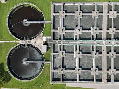
Semiconductor fabrication plants are at the forefront of technological innovation, but this progress comes with significant wastewater management challenges. The complex chemical processes involved in chip manufacturing generate wastewater with a unique and demanding contaminant profile. This includes high concentrations of fluoride (ranging from 50–500 mg/L), significant levels of total organic carbon (TOC, typically 100–1,000 mg/L), a variety of heavy metals such as copper and arsenic, and persistent spent photoresist chemicals. Meeting increasingly stringent local regulatory limits, which can vary dramatically by region and even by fabrication node technology (e.g., 3nm vs. 10nm), is paramount. the global issue of water scarcity, particularly acute in regions like Arizona, Taiwan, and Singapore where many fabs are located, necessitates advanced water recovery and reuse strategies. For instance, evaporative losses in cooling towers can account for 60–80% of total water consumption in many facilities (IRDS 2023). To address these multifaceted demands, generic industrial wastewater treatment systems are often insufficient, requiring specialized engineering solutions. TSMC’s Arizona fab, for example, has demonstrated the feasibility of substantial water savings, reducing its freshwater demand by 30% through on-site recycling initiatives (2024 sustainability report).
| Parameter | Typical Concentration Range | Example Regional Discharge Limits (2024) | Impact of Fab Node |
|---|---|---|---|
| Fluoride | 50–500 mg/L | Taiwan: 10 mg/L EU: 1.0 mg/L |
Higher node complexity may involve more aggressive etching chemistries, potentially increasing fluoride load. |
| Total Organic Carbon (TOC) | 100–1,000 mg/L | Singapore: 5 mg/L U.S. (State-specific): 5 mg/L |
Advanced lithography and cleaning processes can introduce a wider range of organic compounds. |
| Heavy Metals (e.g., Copper, Arsenic) | Trace to significant levels | Taiwan: 0.1 mg/L (Arsenic) Singapore: 0.5 mg/L (Copper), 0.1 mg/L (Arsenic) |
Plating and etching processes are primary sources; newer nodes may utilize novel metallization techniques. |
| Spent Photoresist Chemicals | Variable | Generally regulated under broader organic and hazardous waste categories. | Photoresist formulations evolve with lithography advancements, impacting chemical composition. |
| Total Dissolved Solids (TDS) | Variable (can be high in recycle streams) | Varies significantly by region and receiving water body. | Concentration increases with water recycling due to dissolved salt buildup. |
Water scarcity is a critical driver for advanced treatment. Fabs located in arid regions like Arizona face significant water withdrawal caps, potentially limiting operations for a 300mm fab to around 1.5 million gallons per day. The operational reality is that a substantial portion of this water is not consumed but lost through evaporation. Addressing this requires not just treating wastewater to discharge standards but also maximizing water recovery for reuse within the facility, reducing the demand for fresh water and alleviating pressure on local water resources.
Process Flow Diagrams: 3 System Architectures for Chip Fab Wastewater Treatment
Selecting the appropriate wastewater treatment architecture is a critical engineering decision, directly impacting recovery rates, operational costs, and regulatory compliance. Three primary system architectures are commonly considered for semiconductor fabrication plants: conventional, hybrid, and zero-liquid-discharge (ZLD). Each offers distinct advantages and disadvantages depending on the fab's scale, wastewater characteristics, and specific water reuse objectives.
A conventional system typically begins with wastewater segregation at the source, followed by chemical precipitation to remove heavy metals and suspended solids. This is often coupled with Dissolved Air Flotation (DAF) systems for pretreatment. Subsequent biological treatment, such as activated sludge or Membrane Bioreactors (MBRs), addresses dissolved organic pollutants. Finally, high-pressure Reverse Osmosis (RO) is employed to desalinate the water to meet discharge standards or for limited reuse. Conventional systems can handle flow rates from 50–500 m³/h and typically occupy a footprint of 1,000–3,000 m². However, they generally achieve water recovery rates of only 70–80% and can generate substantial volumes of sludge, leading to high disposal costs.
A hybrid system builds upon conventional methods by integrating more advanced and efficient technologies. This architecture might start with electrocoagulation for effective heavy metal and emulsified oil removal, followed by DAF. MBR systems offer a compact and highly efficient solution for TOC and nitrogen removal, providing a superior effluent quality compared to conventional biological treatment. The treated water then passes through high-recovery RO systems, achieving recovery rates of 90–95%. Emerging technologies like Membrion’s electro-ceramic desalination are also integrated into hybrid designs, offering up to 90% water recovery with a reported 30% lower energy consumption than traditional thermal ZLD systems. This approach balances high recovery with manageable CAPEX and OPEX.
Zero-Liquid-Discharge (ZLD) systems represent the most advanced approach, aiming for nearly complete water recovery. These systems typically involve thermal evaporation followed by crystallization to produce solid salt byproducts. ZLD systems can achieve recovery rates upwards of 98%. For a flow rate of 100 m³/h, the capital expenditure (CAPEX) for a ZLD system can range from $5–10 million, with operational expenditure (OPEX) between $0.5–1.5/m³. While ZLD significantly minimizes freshwater intake and eliminates liquid discharge, its high energy consumption and substantial CAPEX are major considerations. Lam Research data indicates that ZLD systems can reduce freshwater demand by as much as 1.2 million gallons per day for a 300mm fab, highlighting its effectiveness in water-stressed regions.
The process flow for a hybrid system might look like this: Wastewater segregation feeds into an electrocoagulation unit, which removes approximately 95–99% of heavy metals and suspended solids. The effluent then moves to a DAF system for further solids removal (achieving 95% TSS removal). Following DAF, an MBR system targets dissolved organics, removing 80–90% TOC. The final polishing step is high-recovery RO, which can achieve 99% fluoride removal and produce high-quality recycled water. For enhanced pre-treatment before RO, dissolved air flotation is often employed. For the final stage of desalination, especially for high-salinity streams or where extremely high purity is needed, high-recovery RO systems are critical. These systems are designed for maximum water reclamation.
Contaminant Removal Technologies: Efficiency Data and Selection Guide

Effectively treating semiconductor wastewater requires a deep understanding of various contaminant removal technologies, their efficiencies, operational parameters, and cost implications. Selecting the right combination of technologies is crucial for achieving specific discharge limits and water reuse goals. Key contaminants like fluoride, TOC, and heavy metals each present unique treatment challenges.
Fluoride removal is often achieved through chemical precipitation using lime or calcium chloride. This method can achieve 90–95% removal but generates significant volumes of calcium fluoride sludge, typically 0.5–1.0 kg sludge per m³ of treated water, which incurs disposal costs. Reverse Osmosis (RO) is highly effective for fluoride, capable of removing 99% of dissolved fluoride ions. However, RO performance can be sensitive to pH, and optimal fluoride removal is generally achieved at pH 5–6, often requiring upstream pH adjustment.
TOC removal is primarily addressed through biological treatment processes. Membrane Bioreactors (MBRs), for instance, can remove 80–90% of TOC by providing a compact and highly efficient biological treatment environment with long retention times (12–24 hours). For recalcitrant or very high TOC loads, advanced oxidation processes (AOPs) like UV/H₂O₂ can achieve 95% TOC removal. However, AOPs are energy-intensive, with operational costs potentially ranging from $0.2–0.5/m³.
Heavy metals removal, including copper and arsenic, can be effectively managed by electrocoagulation (EC). EC technologies are capable of removing 95–99% of these metals. The primary operational consideration for EC is the need for frequent electrode replacement, typically every 1–2 years, which contributes to OPEX. Ion exchange (IX) is another highly effective method for metals removal, achieving 99% removal. However, the cost of IX resins, which can be $50–100/kg, and the regeneration chemicals contribute significantly to overall treatment costs.
Emerging technologies are also playing a vital role. Membrion’s electro-ceramic desalination offers a high-recovery solution, achieving 90% water recovery while consuming 30% less energy than conventional thermal ZLD systems, making it an attractive option for hybrid architectures. Forward osmosis (FO) is also gaining traction for treating high-salinity wastewater streams, offering a low-energy alternative for pre-concentration before further treatment or disposal.
| Contaminant | Technology | Typical Removal Efficiency (%) | Key Operational Considerations | Estimated Cost Range (OPEX per m³) |
|---|---|---|---|---|
| Fluoride | Chemical Precipitation (Lime/CaCl₂) | 90–95% | High sludge generation (0.5–1.0 kg/m³), requires solids handling. | $0.10–0.30 (chemicals, sludge disposal) |
| Fluoride | Reverse Osmosis (RO) | 99% | Requires pre-treatment, pH adjustment (5–6 optimal), membrane fouling potential. | $0.20–0.50 (energy, membrane replacement) |
| TOC | MBR (Membrane Bioreactor) | 80–90% | Compact footprint, requires membrane cleaning/replacement, biological process stability. | $0.15–0.40 (energy, maintenance) |
| TOC | Advanced Oxidation (UV/H₂O₂) | 95% | High energy consumption, potential for byproduct formation, requires chemical dosing. | $0.20–0.50 (energy, chemicals) |
| Heavy Metals (Cu, As) | Electrocoagulation | 95–99% | Electrode replacement (1–2 years), energy consumption. | $0.15–0.35 (energy, electrode replacement) |
| Heavy Metals (Cu, As) | Ion Exchange | 99% | High resin cost, regeneration chemicals, requires pre-treatment to prevent fouling. | $0.25–0.60 (resin replacement, chemicals) |
Cost Breakdown: CAPEX, OPEX, and ROI for Chip Fab Wastewater Systems
Procurement teams evaluating wastewater treatment systems for semiconductor fabs must conduct a thorough cost-benefit analysis that extends beyond initial equipment purchases to encompass long-term operational expenses and return on investment (ROI). The capital expenditure (CAPEX) and operational expenditure (OPEX) vary significantly based on the chosen system architecture and the fab's capacity. Understanding these costs is crucial for accurate budgeting and justifying investments.
Capital Expenditure (CAPEX) for semiconductor wastewater treatment systems can be substantial. For a conventional system designed for a flow rate of 50 m³/h, CAPEX can range from $1–3 million, covering civil works, equipment procurement, and installation. Hybrid systems, offering higher recovery and advanced treatment, typically have a CAPEX of $3–7 million for a capacity of 100 m³/h. Zero-Liquid-Discharge (ZLD) systems, with their complex thermal evaporation and crystallization units, represent the highest CAPEX, potentially ranging from $5–10 million for a 100 m³/h system.
Operational Expenditure (OPEX) is a critical factor for long-term financial planning. Conventional systems generally have the lowest OPEX, estimated at $0.3–0.8/m³, primarily driven by chemicals, energy, and sludge disposal costs. Hybrid systems, with their advanced technologies and higher recovery rates, typically have OPEX in the range of $0.5–1.2/m³, reflecting increased energy demands and maintenance for more sophisticated equipment. ZLD systems, due to their high energy requirements for evaporation and steam generation, incur the highest OPEX, ranging from $1.0–2.5/m³.
The Return on Investment (ROI) for advanced wastewater treatment systems is driven by several key factors. Significant water savings are a primary driver; a 300mm fab utilizing advanced recycling can reduce freshwater demand by 1.2 million gallons per day, translating to substantial cost avoidance. Regulatory compliance is another critical ROI component, as avoiding daily fines that can range from $10,000–$50,000 for non-compliance is paramount. many regions offer sustainability incentives, such as Taiwan's green fab tax credits, which can further enhance the financial viability of investing in water-efficient technologies. Intel’s Leixlip fab, for example, reported a 20% reduction in OPEX by implementing Membrion’s electro-ceramic desalination technology, showcasing the tangible financial benefits of adopting innovative solutions.
| System Architecture | Typical Flow Rate (m³/h) | Estimated CAPEX ($M) | Estimated OPEX ($/m³) | Key ROI Drivers |
|---|---|---|---|---|
| Conventional | 50 | 1–3 | 0.3–0.8 | Basic regulatory compliance, moderate water savings. |
| Hybrid | 100 | 3–7 | 0.5–1.2 | High water recovery (90–95%), reduced sludge, enhanced compliance, operational flexibility. |
| Zero-Liquid-Discharge (ZLD) | 100 | 5–10 | 1.0–2.5 | Maximum water recovery (98%+), zero liquid discharge, significant water stress mitigation, regulatory certainty. |
Regional Compliance Guide: Discharge Limits and Permitting for Semiconductor Fabs
Navigating the complex landscape of environmental regulations is a critical responsibility for Environmental, Health, and Safety (EHS) managers in the semiconductor industry. Discharge limits for wastewater vary significantly by region, and understanding these requirements is essential for designing compliant treatment systems and avoiding substantial penalties. The permitting process itself can be lengthy and requires meticulous documentation and adherence to local protocols.
Key semiconductor manufacturing hubs have established specific discharge limits. In Taiwan, regulations set by the Environmental Protection Administration (EPA) typically include limits of 10 mg/L for fluoride, 5 mg/L for TOC, and 0.1 mg/L for arsenic (as of 2024). Singapore, through its National Environment Agency (NEA), enforces limits such as 5 mg/L for TOC, 0.5 mg/L for copper, and 0.1 mg/L for arsenic. In the European Union, the Industrial Emissions Directive (IED) 2010/75/EU outlines broad requirements, often with specific country-level implementations that can include limits like 0.1 mg/L for arsenic and 1.0 mg/L for fluoride. In the United States, regulations are primarily state-driven, with the EPA issuing national guidelines. For example, California might have a fluoride limit of 2 mg/L, while Texas could set a TOC limit of 5 mg/L. The EPA's 2024 semiconductor effluent guidelines provide a foundational framework for national standards.
The permitting process for a new or retrofitted fab's wastewater treatment system typically involves several stages and can span 6–12 months. Required documentation often includes detailed engineering reports, process design documents, pilot test data demonstrating treatment efficacy, and environmental impact assessments. Common pitfalls during this process include underestimating the volume and cost of sludge disposal, failing to account for peak flow rates and contaminant loads, and not adequately engaging with local regulatory authorities early in the design phase. A proactive approach, informed by a thorough understanding of regional requirements and robust treatment design, is essential for a smooth permitting journey.
| Region | Fluoride (mg/L) | TOC (mg/L) | Arsenic (mg/L) | Copper (mg/L) | Regulatory Authority (Example) |
|---|---|---|---|---|---|
| Taiwan | 10 | 5 | 0.1 | 0.5 (typical) | Environmental Protection Administration |
| Singapore | N/A (often covered by broader parameters) | 5 | 0.1 | 0.5 | National Environment Agency |
| European Union (General) | 1.0 | N/A (covered by BOD/COD) | 0.1 | 0.5 (typical) | EU Industrial Emissions Directive |
| United States (Example: California) | 2 | N/A (covered by BOD/COD) | 0.05 (typical) | 0.1 (typical) | State Water Resources Control Board |
| United States (Example: Texas) | N/A | 5 | 0.05 (typical) | 0.5 (typical) | Texas Commission on Environmental Quality |
Frequently Asked Questions
What is the best wastewater treatment system for a 3nm semiconductor fab?
For a 3nm semiconductor fab, which typically involves more complex and aggressive chemical processes, a hybrid or Zero-Liquid-Discharge (ZLD) system is recommended. These architectures provide higher water recovery rates (90-98%) and advanced contaminant removal necessary to meet stringent discharge limits and water scarcity mandates. The choice between hybrid and ZLD depends on the specific regional regulations, water stress levels, and the fab's budget for CAPEX and OPEX.
How much does a zero-liquid-discharge (ZLD) system cost for a semiconductor fab?
The cost of a ZLD system for a semiconductor fab can range significantly, but for a capacity of 100 m³/h, expect capital expenditure (CAPEX) between $5–10 million. Operational expenditure (OPEX) for ZLD systems is typically higher than other treatment methods, ranging from $1.0–2.5 per cubic meter, primarily due to high energy consumption for evaporation and steam generation.
What are the fluoride removal options for chip fab wastewater, and which is most cost-effective?
Primary fluoride removal options include chemical precipitation (e.g., lime, calcium chloride) and Reverse Osmosis (RO). Chemical precipitation is cost-effective for bulk removal (90-95%) but generates significant sludge. RO offers higher removal efficiency (99%) and better water quality for reuse but has higher energy costs and requires pre-treatment. For cost-effectiveness, a combination of chemical precipitation followed by RO, or RO alone if pre-treatment is optimized, is often preferred depending on the target fluoride concentration and desired water quality.
Can semiconductor wastewater be recycled for ultra-pure water (UPW) production?
Yes, with advanced treatment, semiconductor wastewater can be recycled for ultra-pure water (UPW) production. This typically involves a multi-stage process including high-efficiency RO, ion exchange, and advanced polishing steps to remove residual ions and contaminants. Achieving UPW quality from wastewater requires sophisticated treatment trains and rigorous quality control to meet the extremely low conductivity and impurity requirements of semiconductor manufacturing.
What are the key regulatory limits for semiconductor wastewater discharge in Taiwan and Singapore?
In Taiwan, key limits include 10 mg/L for fluoride, 5 mg/L for TOC, and 0.1 mg/L for arsenic. Singapore's regulations often specify 5 mg/L for TOC, 0.5 mg/L for copper, and 0.1 mg/L for arsenic. These limits are subject to updates, and EHS managers should consult the latest official guidelines from their respective environmental protection agencies.
Related Equipment
The following Zhongsheng Environmental products are engineered for the wastewater challenges discussed above:
- DAF systems for semiconductor wastewater pretreatment — view specifications, capacity range, and technical data
- high-recovery RO systems for semiconductor water recycling — view specifications, capacity range, and technical data
- MBR systems for TOC and nitrogen removal in semiconductor wastewater — view specifications, capacity range, and technical data
Need a customized solution? Request a free quote with your specific flow rate and pollutant parameters.