Why Semiconductor Developer Wastewater Requires Specialized Treatment
Semiconductor developer wastewater presents a unique and formidable challenge for industrial wastewater treatment systems. Unlike general industrial effluents, developer wastewater is characterized by high concentrations of photoresists, organic solvents such as propylene glycol monomethyl ether acetate (PGMEA), and potentially toxic heavy metals like copper and arsenic. These contaminants can be present at levels 10 to 100 times higher than in other semiconductor fab streams, according to SEMATECH 2024 data. Meeting the increasingly stringent regulatory discharge limits for 2025, which include targets like Total Suspended Solids (TSS) below 30 mg/L, Chemical Oxygen Demand (COD) below 125 mg/L, copper below 0.1 mg/L, and arsenic below 0.01 mg/L (as stipulated by EPA and EU Industrial Emissions Directive 2010/75/EU), necessitates advanced and specialized treatment methodologies.
Failure to adequately treat developer wastewater can lead to significant environmental and operational risks. Untreated or inadequately treated effluent can cause severe membrane fouling in downstream water reuse systems, leading to increased operational costs and reduced system lifespan. non-compliance with discharge regulations can result in substantial fines, reputational damage, and even operational shutdowns. For instance, a 10 million gallon per day (MGD) fab in Taiwan, as documented in a 2024 case study, successfully reduced COD from 800 mg/L to under 50 mg/L by implementing a combination of advanced oxidation and membrane filtration, demonstrating the efficacy of targeted treatment strategies.
| Contaminant Type | Typical Concentration Range | Regulatory Limit (2025, Example) | Treatment Challenge |
|---|---|---|---|
| Photoresists (e.g., Novolak resins) | 500 - 2,000 mg/L | N/A (Indirectly via COD/TSS) | High organic load, can cause foaming and fouling. |
| Organic Solvents (e.g., PGMEA, NMP) | 200 - 1,500 mg/L (PGMEA), 100 - 800 mg/L (NMP) | COD < 125 mg/L | High COD, volatile organic compounds (VOCs), can be inhibitory to biological processes. |
| Heavy Metals (e.g., Copper, Arsenic) | 5 - 50 mg/L (Copper), 0.1 - 5 mg/L (Arsenic) | Copper < 0.1 mg/L, Arsenic < 0.01 mg/L | Toxicity to aquatic life, potential for bioaccumulation, requires specific removal technologies. |
| Total Suspended Solids (TSS) | 100 - 2,000 mg/L | TSS < 30 mg/L | Can include fine particles from photoresists and etching processes, requiring effective physical separation. |
Contaminant Profile: What’s in Semiconductor Developer Wastewater?
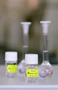
Understanding the precise composition of semiconductor developer wastewater is paramount for designing an effective treatment strategy. This stream is a complex cocktail, primarily originating from the photolithography process, where developers are used to selectively remove exposed or unexposed photoresist. Common contaminants include photoresists themselves, often complex organic polymers like novolak resins, typically found in concentrations ranging from 500 to 2,000 mg/L. Organic solvents, critical for dissolving and dispersing these resists, are also present in high quantities. Propylene glycol monomethyl ether acetate (PGMEA) can range from 200 to 1,500 mg/L, while N-Methyl-2-pyrrolidone (NMP), another common solvent, can be present at 100 to 800 mg/L. These organic components contribute significantly to the high Chemical Oxygen Demand (COD) of the wastewater.
heavy metals, often introduced during etching or as part of resist formulations, pose a significant challenge. Copper concentrations can range from 5 to 50 mg/L, and arsenic, though less common in developer streams specifically, can be present at 0.1 to 5 mg/L depending on the fab's processes and wafer types. Total Suspended Solids (TSS), comprising fine photoresist particles, etching residues, and precipitated materials, can fluctuate wildly from 100 to 2,000 mg/L. This inherent variability, coupled with pH levels that can span from highly acidic (pH 2) to highly alkaline (pH 12), underscores the necessity for robust, modular, and adaptable treatment systems capable of handling diverse influent conditions.
| Contaminant | Typical Concentration Range (mg/L) | Primary Source in Fab | Key Treatment Considerations |
|---|---|---|---|
| Photoresists (Polymers) | 500 - 2,000 | Photolithography (Developer Rinse) | High COD, potential for foaming, requires effective physical separation and oxidation. |
| PGMEA (Propylene Glycol Monomethyl Ether Acetate) | 200 - 1,500 | Photolithography (Developer Solvent) | High COD, VOC, requires advanced oxidation or specialized biological treatment (if diluted). |
| NMP (N-Methyl-2-pyrrolidone) | 100 - 800 | Photolithography (Developer Solvent) | High COD, VOC, potential reproductive toxicity, requires advanced oxidation. |
| Copper (Cu) | 5 - 50 | Etching, Resist Components | Toxic, requires chemical precipitation, ion exchange, or selective adsorption. |
| Arsenic (As) | 0.1 - 5 | Etching, Resist Components (Less common in developer) | Highly toxic, requires specific chemical precipitation or adsorption. |
| TSS (Total Suspended Solids) | 100 - 2,000 | Photoresist particles, etching residues | Requires effective clarification, coagulation, and flocculation. |
| pH | 2 - 12 | Developer formulations, cleaning agents | Requires precise pH adjustment for downstream processes and contaminant removal. |
For more detailed information on heavy metal removal, refer to our Semiconductor Heavy Metal Wastewater Treatment: Engineering Specs, Cost Data & Process Selection Guide 2025.
Treatment Technologies: How to Remove Contaminants from Developer Wastewater

Addressing the complex contaminant profile of semiconductor developer wastewater demands a multi-barrier approach utilizing advanced treatment technologies. Advanced Oxidation Processes (AOPs) are highly effective for degrading persistent organic compounds like photoresists and solvents. Technologies such as UV/H₂O₂ or ozonation can achieve 90-98% COD removal. For UV/H₂O₂, typical process parameters include a UV dose of 500-1,000 mJ/cm² and an H₂O₂ dosage of 100-500 mg/L, depending on the organic load (enviolet 2024 data). These processes generate highly reactive hydroxyl radicals that mineralize organic pollutants.
Membrane filtration, particularly Reverse Osmosis (RO) and Nanofiltration (NF), plays a crucial role in removing dissolved salts, heavy metals, and remaining suspended solids, achieving 95-99% removal rates. High-recovery RO systems, as highlighted in top-ranking content, can achieve 85-95% water recovery but necessitate robust pretreatment to prevent membrane fouling from organic matter and scaling. Chemical precipitation remains a cost-effective method for heavy metal removal. For instance, copper can be precipitated effectively by adjusting pH to 8-10, achieving 90-99% removal. Arsenic removal typically requires pH adjustment to 6-8, often in conjunction with iron salts to aid co-precipitation.
While biological treatment methods are standard for many industrial wastewaters, their effectiveness for raw developer wastewater is limited due to the high concentrations of organic solvents and potential toxicity, which can inhibit microbial activity. However, biological processes can be employed as a polishing step for significantly pre-treated or diluted streams, or in specialized configurations like membrane bioreactors (MBRs) after substantial organic load reduction. Dissolved Air Flotation (DAF) is an excellent pretreatment step for removing suspended solids and emulsified oils, significantly reducing the load on subsequent treatment stages. For more on DAF, consult our guide on DAF Clarifier Explained.
| Technology | Primary Contaminant Removal | Typical Removal Efficiency | Key Process Parameters/Considerations |
|---|---|---|---|
| Advanced Oxidation Processes (AOPs: UV/H₂O₂, Ozone) | Organic Solvents, Photoresists (COD) | 90-98% COD | UV Dose: 500-1000 mJ/cm², H₂O₂ Dosage: 100-500 mg/L, Ozone Dosage: 5-20 mg/L. Requires careful control of pH and oxidant dosage. |
| Membrane Filtration (RO, NF) | Heavy Metals, Dissolved Salts, TSS | 95-99% (Metals), 98-99.5% (Salts) | Requires extensive pretreatment to prevent fouling and scaling. High-recovery systems achieve 85-95% water recovery. |
| Chemical Precipitation | Heavy Metals (Cu, As, Ni, etc.) | 90-99% | pH adjustment critical (e.g., pH 8-10 for Cu, pH 6-8 for As). Often requires coagulants and flocculants. |
| Dissolved Air Flotation (DAF) | TSS, FOG (Fats, Oils, Grease) | 70-90% TSS, 60-80% FOG | Effective for removing suspended and emulsified contaminants. Often used as pretreatment. |
| Ion Exchange | Specific Heavy Metals (e.g., Copper, Nickel) | >99% | Selective removal of target ions. Requires regeneration of resin. |
| Activated Carbon Adsorption | Trace Organics, Color | >95% | Polishing step for removing residual dissolved organics and color. Requires periodic replacement of carbon. |
For related technologies, see our insights on FGD Scrubbers and Tertiary Wastewater Treatment.
Process Flow Design: Step-by-Step Blueprint for Developer Wastewater Treatment
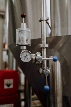
A robust process flow for semiconductor developer wastewater treatment integrates multiple stages to ensure comprehensive contaminant removal and enable water reuse or Zero Liquid Discharge (ZLD). The initial step is Pretreatment, focusing on pH adjustment and the removal of gross solids. This typically involves chemical addition for pH correction (e.g., using sulfuric acid or caustic soda) and coagulation/flocculation to destabilize and aggregate suspended particles. Typical coagulants like ferric chloride or polyaluminum chloride (PAC) are dosed at 50-200 mg/L, followed by flocculants to enhance particle settling. PLC-controlled chemical dosing systems ensure precise application of these chemicals.
Following pretreatment, Primary Treatment often employs Dissolved Air Flotation (DAF) or sedimentation to remove a significant portion of suspended solids (70-90%) and floatable oils and grease (FOG). Our ZSQ series DAF system, for example, is designed for efficient separation of these contaminants. The next critical stage is Secondary Treatment, where dissolved organics and heavy metals are targeted. This typically involves Advanced Oxidation Processes (AOPs) to break down complex organics and membrane filtration (e.g., RO/NF) for heavy metal and dissolved solids removal. Process parameters like UV dose for AOPs and membrane flux for RO are carefully controlled.
Tertiary Treatment serves as a polishing step to remove any remaining trace contaminants and meet stringent water quality requirements for reuse. Technologies such as ion exchange can achieve >99% removal of specific heavy metals like copper, while activated carbon adsorption effectively removes residual dissolved organic compounds and color. The final stage is Zero Liquid Discharge (ZLD) or advanced water reuse. This involves processes like evaporation and crystallization to recover all water and concentrate the remaining solids into a manageable form. High-recovery RO systems, as discussed in industry guides, play a vital role in maximizing water recovery before evaporation.
A typical process flow sequence would be: Pretreatment (pH Adjustment, Coagulation/Flocculation) → Primary Treatment (DAF/Sedimentation) → Secondary Treatment (AOPs, Membrane Filtration) → Tertiary Treatment (Ion Exchange, Activated Carbon) → ZLD/Water Reuse (Evaporation, Crystallization).
Consider using an automatic chemical dosing system for precise chemical application throughout the process. For high-purity water reuse, explore our industrial Reverse Osmosis (RO) water treatment systems.
Cost Breakdown: CAPEX, OPEX, and ROI for Semiconductor Wastewater Treatment
The capital expenditure (CAPEX) for a comprehensive semiconductor developer wastewater treatment system, especially one designed for Zero Liquid Discharge (ZLD), can be substantial. For a complete ZLD system capable of treating wastewater from a large fab (10 MGD), CAPEX can range from $10 million to $15 million. Smaller fabs or those with less ambitious reuse targets might see CAPEX in the range of $2.5 million to $5 million for a system treating around 1 MGD. These figures are based on industry benchmarks and typical project scopes for advanced treatment trains, including AOPs, multi-stage membrane filtration, and evaporation/crystallization units.
Operating expenditures (OPEX) for treating semiconductor wastewater typically fall between $0.50 to $2.00 per cubic meter ($1.90 to $7.60 per 1,000 gallons) of wastewater treated. This includes costs for energy (pumping, UV lamps, evaporators), chemicals (acids, bases, coagulants, oxidants), consumables (membranes, activated carbon), labor, and maintenance. The exact OPEX is highly dependent on the chosen treatment technologies, the influent wastewater characteristics, and the level of automation. Energy consumption, particularly for AOPs and ZLD evaporation stages, is often the largest component of OPEX.
The Return on Investment (ROI) for such systems is driven by several factors. Water savings are a primary driver, with recovered water potentially valued at $0.50 to $1.50 per cubic meter, depending on local water costs. Avoiding regulatory fines, which can be up to $100,000 per violation, represents significant indirect savings. achieving sustainability goals, such as a 30% reduction in freshwater demand, enhances corporate social responsibility and brand image. A notable case example involves a 5 MGD fab in Arizona that achieved a 3-year ROI by implementing a system with 90% water reuse, significantly reducing their reliance on municipal water supplies.
| Cost Component | Typical Range (for 1-10 MGD fab) | Key Drivers | ROI Contribution |
|---|---|---|---|
| CAPEX (Total System) | $2.5M - $15M | Fab size, treatment complexity (ZLD vs. reuse), technology selection. | Initial investment for long-term savings. |
| OPEX (per m³ treated) | $0.50 - $2.00 | Energy consumption, chemical usage, labor, maintenance, consumables. | Ongoing costs managed through process optimization and energy efficiency. |
| Water Savings | $0.50 - $1.50 per m³ recovered | Local water utility rates, volume of water reused. | Direct revenue/cost reduction from water reuse. |
| Regulatory Compliance | Avoidance of fines ($10K - $100K+ per violation) | Stringency of local discharge permits, historical compliance record. | Risk mitigation and avoidance of significant financial penalties. |
| Sustainability Goals | Enhanced brand reputation, reduced environmental footprint | Corporate ESG targets, public perception. | Indirect value, market access, investor relations. |
For a detailed financial perspective, see our article on Wafer Fab Wastewater Treatment Cost.
Zero-Liquid Discharge (ZLD) for Semiconductor Fabs: Design and Implementation
Implementing a Zero Liquid Discharge (ZLD) system for semiconductor developer wastewater is the ultimate solution for achieving complete regulatory compliance and maximizing water circularity. A typical ZLD system is an integration of multiple advanced treatment stages. It begins with robust pretreatment, including DAF and chemical precipitation, to remove solids and heavy metals. This is followed by high-efficiency membrane filtration, such as multi-stage RO or NF, to further purify the water and achieve high water recovery rates, often exceeding 90%. The brine concentrate from the membranes then proceeds to the evaporation and crystallization stages.
The choice of evaporation technology is critical for energy efficiency. Mechanical Vapor Recompression (MVR) evaporators are often preferred over traditional thermal evaporators, offering energy savings of 50-70% by recycling latent heat. Crystallizers then further concentrate the brine, producing solid salts that can be disposed of or, in some cases, repurposed. Hybrid systems, such as Forward Osmosis (FO) integrated with NF, are also gaining traction for their ability to handle challenging brines and achieve higher water recovery with potentially lower energy footprints compared to conventional RO alone. The design must account for the specific characteristics of the developer wastewater, including its high organic load and variable pH, which can impact membrane longevity and fouling rates.
While ZLD systems significantly increase CAPEX by an estimated 30-50% compared to conventional discharge systems, they offer substantial long-term benefits. These include the complete elimination of discharge fees, which can be considerable in regions with strict regulations. by achieving 80-90% water recovery, ZLD drastically reduces freshwater intake costs. The design and implementation of a ZLD system require meticulous planning, considering factors like plant footprint, energy availability, and the management of concentrated solid waste streams. For more on ZLD strategies, consult our Semiconductor Wastewater Zero Liquid Discharge: Engineering Specs, Cost Data & Hybrid System Design 2025.
Frequently Asked Questions
What are the primary contaminants in semiconductor developer wastewater?
The primary contaminants include high concentrations of photoresists, organic solvents like PGMEA and NMP, and heavy metals such as copper and arsenic. These contribute to high COD, TSS, and potential toxicity.
Are biological treatment methods suitable for developer wastewater?
Generally, biological treatment is less effective for raw developer wastewater due to high organic loads and potential toxicity. It may be used as a polishing step after significant pre-treatment or in specialized configurations for diluted streams.
What is the typical removal efficiency for AOPs in treating developer wastewater?
Advanced Oxidation Processes (AOPs) like UV/H₂O₂ or ozonation can achieve 90-98% removal of organic contaminants, significantly reducing COD and breaking down complex organic molecules.
How does ZLD help semiconductor fabs comply with 2025 regulations?
ZLD systems eliminate wastewater discharge entirely, ensuring compliance with all discharge limits for TSS, COD, heavy metals, and other regulated parameters, thereby preventing fines and operational disruptions.
What is the role of membrane filtration in developer wastewater treatment?
Membrane filtration, particularly RO and NF, is crucial for removing dissolved heavy metals, salts, and residual suspended solids, achieving high water recovery rates for reuse or further concentration in ZLD systems.
Related Equipment
- ZSQ series DAF system for semiconductor wastewater pretreatment — view specifications, capacity range, and technical data
Need a customized solution? Request a free quote with your specific flow rate and pollutant parameters.