Why Semiconductor Heavy Metal Wastewater Treatment is a $2.5B Challenge in 2025
Semiconductor fabs generate wastewater with copper concentrations up to 500 mg/L—far exceeding EPA discharge limits of 1.3 mg/L (40 CFR 469). Advanced treatment processes like electrochemical deposition (ECD) and membrane bioreactors (MBR) achieve 99%+ copper removal with no sludge, while chemical precipitation remains the most cost-effective for arsenic and fluoride. This guide provides engineering specs, cost data, and a decision framework for selecting the optimal process based on fab size, metal profile, and sustainability goals.
Global semiconductor fab water consumption is projected to reach 1.5 trillion liters per year by 2025, underscoring the escalating challenge of managing wastewater. Regulatory bodies and environmental consciousness are driving stricter compliance, with copper discharge violations alone costing fabs an estimated $250,000 to $1,000,000 annually in fines, according to EPA NPDES enforcement data. Regions like Taiwan and South Korea are leading the charge in water reuse mandates, requiring new fabs to achieve over 80% water recovery (ITRI 2025 report). A real-world example illustrates the stakes: a 300mm fab in Arizona faced $800,000 in fines for copper exceedances, prompting a $3.2 million retrofit with an Electrochemical Deposition (ECD) system to ensure future compliance.
Contaminant Profile: What’s in Semiconductor Wastewater and Why It’s Hard to Treat
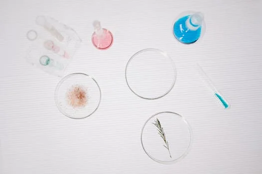
Understanding the complex composition of semiconductor wastewater is crucial for selecting effective treatment technologies. Chemical-Mechanical Planarization (CMP) processes are a significant contributor, generating up to 60% of fab wastewater and often containing copper concentrations ranging from 100 to 500 mg/L (ElectraMet case study). Etching processes introduce other challenging contaminants, including arsenic, with concentrations typically between 5 and 50 mg/L, and fluoride, often in the range of 100 to 1,000 mg/L (GL Environment data). Many semiconductor wastewater streams also originate from acid waste, such as sulfuric or piranha solutions, leading to very low pH levels of 1 to 3, necessitating effective neutralization prior to further treatment (BW Water). the high salinity, with Total Dissolved Solids (TDS) often ranging from 5,000 to 20,000 mg/L, can pose significant challenges for membrane-based treatment processes, impacting their performance and longevity (Membrion ECD limitations).
| Process Step | Typical Contaminant | Typical Concentration Range (mg/L) |
|---|---|---|
| CMP | Copper | 100 - 500 |
| Etching | Arsenic | 5 - 50 |
| Etching | Fluoride | 100 - 1,000 |
| Acid Waste Streams | Acids (e.g., Sulfuric) | Low pH (1-3) |
| Rinsing/General | TDS | 5,000 - 20,000 |
| Lithography | Various Organics | Variable |
Regulatory Limits for Heavy Metals in Semiconductor Wastewater: EPA, EU, and Asian Standards
Compliance with stringent regulatory limits for heavy metals in wastewater discharge is paramount for semiconductor fabs. In the United States, the EPA's 40 CFR 469 sets specific effluent limitations, including a maximum of 1.3 mg/L for copper and 0.1 mg/L for arsenic, with fluoride limited to 4 mg/L (daily maximum). The European Union's Industrial Emissions Directive (IED) 2010/75/EU often imposes even stricter limits for new facilities, with copper discharges potentially capped at 0.5 mg/L. Asian nations are also implementing aggressive water management policies. Taiwan's 2025 mandate requires zero liquid discharge (ZLD) for fabs exceeding 10,000 square meters, while South Korea aims for 90% water reuse in new fabs, as stipulated by the Ministry of Environment in 2024. China is also progressively tightening its discharge standards for industrial wastewater.
| Region/Authority | Copper (mg/L) | Arsenic (mg/L) | Fluoride (mg/L) | Notes |
|---|---|---|---|---|
| EPA (USA) | 1.3 (max) | 0.1 (max) | 4 (daily max) | 40 CFR 469 |
| EU IED | 0.5 (new fabs) | 0.05 (new fabs) | 10 (new fabs) | Best Available Techniques (BAT) Reference Document |
| Taiwan EPA | < 0.5 (target) | < 0.05 (target) | < 5 (target) | ZLD mandate for large fabs (>10,000 m²) |
| South Korea MOE | < 0.5 (target) | < 0.05 (target) | < 5 (target) | 90% water reuse mandate for new fabs |
| China MEP | < 0.5 (regional) | < 0.1 (regional) | < 10 (regional) | Varies by industry and region |
Treatment Process Deep Dive: How Each Technology Handles Copper, Arsenic, and Fluoride
Selecting the appropriate treatment technology hinges on the specific contaminants present and the desired removal efficiencies. Chemical precipitation is a well-established method, offering low Capital Expenditure (CAPEX) in the range of $50–$150 per cubic meter of treated water. However, its primary drawbacks include significant sludge generation, which requires costly disposal, and moderate copper removal efficiencies of 80–90% (GL Environment). For high-purity copper recovery and zero sludge generation, Electrochemical Deposition (ECD) stands out, achieving over 99% copper removal. While effective, ECD typically incurs higher Operational Expenditure (OPEX) of $0.20–$0.50 per cubic meter due to energy consumption (Membrion case study). Membrane Bioreactors (MBR) can achieve up to 95% copper removal, but their performance can be significantly impacted by high TDS levels common in semiconductor wastewater, leading to fouling issues (Zhongsheng MBR limitations). Ion exchange is highly effective for removing arsenic, with removal efficiencies reaching 99%, but the cost of resin regeneration can range from $0.30 to $0.80 per cubic meter of treated water (BW Water). Often, a hybrid approach combining technologies offers the optimal solution. For instance, chemical precipitation followed by ECD can efficiently manage copper, while ion exchange can be employed for targeted arsenic removal. A typical hybrid system for a 500 m³/day fab might involve a CAPEX of approximately $2.1 million.
| Process | Copper Removal Efficiency (%) | Arsenic Removal Efficiency (%) | Fluoride Removal Efficiency (%) | Sludge Generation | Estimated OPEX ($/m³) |
|---|---|---|---|---|---|
| Chemical Precipitation | 80 - 90 | 70 - 85 | 60 - 75 | High | $0.10 - $0.30 |
| Electrochemical Deposition (ECD) | >99 | N/A (for copper) | N/A | None | $0.20 - $0.50 |
| MBR | 95 | Variable (depends on biomass) | Variable | Low (biomass) | $0.15 - $0.35 |
| Ion Exchange | Variable | >99 | Variable | Low (spent resin) | $0.30 - $0.80 (regeneration) |
| Hybrid (e.g., Chem + ECD + IX) | >99 | >99 | Optimized | Low to Moderate | $0.30 - $0.70 |
For facilities looking to manage complex contaminant profiles and achieve high levels of water purity, advanced solutions like MBR systems for semiconductor wastewater reuse offer a robust option. These systems, combined with other treatment stages, can be tailored to meet the most demanding discharge and reuse requirements.
Cost Breakdown: CAPEX, OPEX, and ROI for Semiconductor Wastewater Treatment Systems
The investment in semiconductor heavy metal wastewater treatment systems can vary significantly based on the chosen technology, fab size, and desired treatment level. Capital Expenditure (CAPEX) for systems treating 100 to 1,000 cubic meters per day typically ranges from $1 million to $5 million, according to SEMI 2025 cost surveys. Operational Expenditure (OPEX) components include chemical costs, which can range from $0.10 to $0.40 per cubic meter for precipitation and neutralization processes, and energy consumption, often between $0.05 and $0.20 per cubic meter, particularly for electrochemical and membrane-based systems (ElectraMet data). Sludge disposal costs can add an additional $0.02 to $0.10 per cubic meter for technologies that generate solid waste (GL Environment data). The Return on Investment (ROI) for these systems is driven by several factors, most notably the recovery of valuable metals like copper, which can be worth approximately $9,000 per ton. significant savings are realized through water reuse, with reductions of $2 to $5 per cubic meter in water-scarce regions. A case study of a 300 m³/day ECD system demonstrated a payback period of just 3.2 years, primarily through copper recovery and substantial water reuse savings.
| Fab Size (m³/day) | Estimated CAPEX ($M) | Estimated OPEX ($/m³) | Typical Payback Period (Years) |
|---|---|---|---|
| 100 | 1.0 - 2.5 | 0.20 - 0.45 | 4 - 7 |
| 500 | 2.0 - 4.0 | 0.25 - 0.60 | 3 - 5 |
| 1,000 | 3.5 - 5.0+ | 0.30 - 0.70 | 2.5 - 4.5 |
How to Select the Right Process for Your Fab: A Decision Framework
Navigating the complexities of semiconductor wastewater treatment requires a systematic approach. The first step involves thoroughly profiling your wastewater stream: accurately measuring metal concentrations, flow rates, and pH levels, using data from tables like the one provided earlier. Next, identify all applicable regulatory requirements, including local discharge limits and any regional water reuse mandates. Concurrently, evaluate your facility's sustainability goals, such as targets for sludge reduction or water reuse percentages. With this information, compare the CAPEX and OPEX of shortlisted technologies against your allocated budget, referencing the cost comparison table. Crucially, pilot testing shortlisted processes at your specific site is essential to validate performance and operational feasibility. A fab in Singapore, for example, conducted a six-month pilot study comparing ECD and chemical precipitation before making its final selection, mitigating risks and ensuring optimal long-term performance.
The decision tree below provides a visual guide:
Which Process is Best for Your Fab?
- Primary Metal of Concern?
- Copper-dominant: Consider ECD for high purity and zero sludge, or Chemical Precipitation for lower CAPEX.
- Arsenic-dominant: Ion exchange is highly effective.
- Fluoride-dominant: Advanced precipitation or adsorption methods may be required.
- Mixed Metals: Hybrid systems are often necessary.
- Fab Size & Flow Rate?
- Small ( < 200 m³/day): Modular systems or optimized chemical precipitation may suffice.
- Medium (200-800 m³/day): ECD, MBR, or advanced chemical treatment become more viable.
- Large ( > 800 m³/day): Integrated and automated systems, potentially with significant reuse capabilities, are essential.
- Budget Constraints?
- Low CAPEX Priority: Chemical precipitation is often the starting point, but consider long-term OPEX.
- Balanced CAPEX/OPEX: ECD and MBR offer better long-term cost efficiency for specific metals.
- High CAPEX Tolerance for Performance/Sustainability: ECD, advanced hybrid systems, and RO for reuse.
- Sustainability Goals?
- Zero Sludge: ECD is the clear choice.
- High Water Reuse (>80%): Requires robust treatment (ECD, RO, MBR) and potentially tertiary polishing.
- Resource Recovery: Focus on technologies that recover valuable metals like ECD.
For advanced water reuse applications, RO systems for semiconductor water reuse can be integrated as a final polishing step to achieve ultra-pure water suitable for process use.
Frequently Asked Questions
What is the most cost-effective way to remove copper from semiconductor wastewater?
For facilities prioritizing low CAPEX and managing moderate copper levels, chemical precipitation is often the most cost-effective initial approach. However, for achieving high removal efficiencies (99%+) and eliminating sludge disposal costs, Electrochemical Deposition (ECD) offers superior long-term cost-effectiveness, despite a higher initial investment.
Can semiconductor wastewater be reused in the fab?
Yes, semiconductor wastewater can be reused. Advanced treatment processes such as ECD, which recovers metals and produces clean effluent, and Reverse Osmosis (RO) systems can achieve 80-95% water recovery. For example, Membrion's ECD technology has demonstrated significant water reuse potential in semiconductor applications.
What are the EPA limits for heavy metals in semiconductor wastewater?
Under EPA 40 CFR 469, the primary limits for semiconductor wastewater discharge are 1.3 mg/L for copper, 0.1 mg/L for arsenic, and 4 mg/L for fluoride (daily maximum).
How much does a semiconductor wastewater treatment system cost?
The cost of a semiconductor wastewater treatment system typically ranges from $1 million to $5 million for flow rates between 100 to 1,000 m³/day. The final cost depends heavily on the chosen treatment process, the specific contaminants, and the required effluent quality.
What are the drawbacks of chemical precipitation for heavy metals?
The primary drawbacks of chemical precipitation include the generation of significant amounts of hazardous sludge that requires costly disposal, higher chemical consumption for pH adjustment and flocculation, and generally lower removal efficiencies compared to advanced technologies, particularly for complex or trace metal removal. For managing the sludge generated by chemical precipitation processes, plate frame filter presses are commonly employed for dewatering.
Related Equipment
- precise chemical dosing for pH adjustment and metal precipitation — view specifications, capacity range, and technical data
Need a customized solution? Request a free quote with your specific flow rate and pollutant parameters.