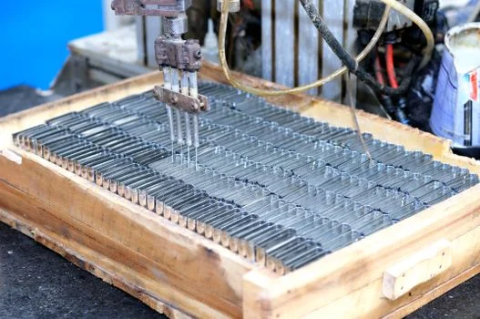
Why Electronics Wastewater Requires Specialized Treatment
Electronics manufacturing wastewater contains high-risk pollutants like tetramethylammonium hydroxide (TMAH), ammonia, and heavy metals (copper, nickel), requiring specialized treatment to meet discharge limits such as the EPA’s 40 CFR Part 469 for semiconductor effluents. For a semiconductor fab manager, the realization that TMAH levels have exceeded regulatory limits often comes too late, resulting in five-figure daily fines and forced operational shutdowns. Generic industrial wastewater systems typically fail in these environments because they cannot address the specific molecular stability of organic developers or the extreme solubility of chelated heavy metals used in PCB etching.
Tetramethylammonium hydroxide (TMAH) serves as the primary organic pollutant of concern in semiconductor and display panel manufacturing. Used extensively as a developer and etchant, TMAH exhibits high aquatic toxicity with an LC50 (lethal concentration to 50% of a population) of approximately 20 mg/L for aquatic life, according to the EPA ECOTOX database. Unlike simple organics, TMAH is resistant to standard activated sludge processes because it acts as a microbial inhibitor at high concentrations. its high alkalinity can destabilize the pH of biological reactors, leading to biomass washout.
Inorganic pollutants present a different challenge. In PCB manufacturing, rinse water often contains 10–100 mg/L of copper and nickel, often in chelated forms that bypass simple hydroxide precipitation. Fluoride, utilized in wafer cleaning, frequently reaches concentrations of 500–1,000 mg/L, far exceeding the 2–4 mg/L discharge limits set by many municipal authorities. Conventional treatment fails because these pollutants require a multi-stage approach: chemical oxidation (such as Fenton’s reagent) to break down organic complexes, followed by specialized precipitation or membrane separation.
| Industry Segment | Primary Pollutants | Typical Concentrations | Regulatory Limit (Avg) |
|---|---|---|---|
| Semiconductor Fabs | TMAH, Fluoride, Ammonia | TMAH: 50–500 mg/L; F: 500 mg/L | TMAH: <1 mg/L; F: <10 mg/L |
| PCB Manufacturing | Copper, Nickel, Lead, COD | Cu: 10–100 mg/L; COD: 500 mg/L | Cu: <0.5 mg/L; Ni: <0.1 mg/L |
| Display Panels (TFT-LCD) | TMAH, Ammonia, Phosphorus | NH3: 100–300 mg/L; P: 20 mg/L | NH3: <5 mg/L; P: <0.5 mg/L |
Treatment Train Comparison: DAF vs. MBR vs. Hybrid Systems for Electronics Wastewater
Selecting the correct treatment train requires balancing the removal of suspended solids (TSS) with the elimination of dissolved organics and nitrogenous compounds. Dissolved Air Flotation (DAF) is the industry standard for primary clarification in electronics plants, particularly for removing photoresist residues and fats, oils, and grease (FOG). DAF systems for TSS and FOG removal in electronics wastewater achieve 92–97% TSS removal by utilizing micro-bubbles to buoy particles to the surface. These systems typically operate at hydraulic loading rates of 4–6 m/h and require precise automated chemical dosing for coagulants and antiscalants in electronics wastewater treatment, such as 5–10 mg/L of polyaluminum chloride (PAC), to ensure effective flocculation.
For dissolved organic removal and nitrification, Membrane Bioreactors (MBR) offer a significant upgrade over traditional clarifiers. MBR systems for COD and ammonia removal in semiconductor wastewater utilize submerged PVDF membranes with a 0.1 μm pore size. This physical barrier ensures that slow-growing nitrifying bacteria are retained within the system, allowing for complete ammonia-to-nitrate conversion even in the presence of inhibitory substances. MBRs in this sector typically maintain flux rates of 15–25 LMH (liters per square meter per hour) with energy consumption ranging from 0.5 to 1.0 kWh/m³.
The most robust solution for modern fabs is the hybrid system (DAF + MBR + RO). This configuration is essential for PCB wastewater treatment systems with zero-discharge designs. In a hybrid train, the DAF removes bulk solids, the MBR degrades TMAH and ammonia (achieving >99% removal), and the RO systems for zero-liquid discharge and water reuse in electronics plants provide the final polishing. RO recovery rates for semiconductor brines typically range from 75–85%, significantly reducing the volume of waste requiring evaporation or off-site disposal.
| Treatment Train | TMAH Removal (%) | COD Removal (%) | Footprint (m²/100 m³/d) | CAPEX ($/m³/d) |
|---|---|---|---|---|
| Standalone DAF | <15% | 30–50% | 25–40 | $1,500–$2,500 |
| Standalone MBR | 85–95% | 90–95% | 40–60 | $3,500–$5,500 |
| Hybrid (DAF+MBR+RO) | >99.5% | >98% | 80–120 | $8,000–$12,000 |
Engineering Specs for Zero-Discharge Electronics Wastewater Systems
Engineering a zero-liquid discharge (ZLD) system for electronics requires precise hydraulic and kinetic modeling to prevent membrane fouling and ensure consistent effluent quality. For the primary DAF stage, the surface loading rate must be maintained between 4 and 6 m/h, with an air-to-solids ratio of 0.02–0.05. This ensures that even light photoresist flocs are effectively separated. Sludge production in these stages typically ranges from 0.5 to 1.0 kg of dry solids per m³ of treated wastewater, necessitating high-capacity high-efficiency sedimentation tanks or filter presses for dewatering.
In the MBR stage, maintaining a Mixed Liquor Suspended Solids (MLSS) concentration between 8,000 and 12,000 mg/L is critical for treating high-strength TMAH streams. High MLSS levels provide a buffer against toxic shocks, but they require significant aeration demand, typically 0.3–0.5 m³ of air per m³ of wastewater. The use of fine-bubble diffusers is mandatory to maximize oxygen transfer efficiency. For nitrogen removal, the hydraulic retention time (HRT) is usually split between an anoxic zone (2–4 hours) and an aerobic zone (6–8 hours) to facilitate denitrification.
The RO and brine management stage is where water recovery is maximized. To achieve 75–85% recovery, RO systems must operate at pressures between 40 and 60 bar, with antiscalant dosing maintained at 2–5 mg/L to prevent calcium fluoride scaling on the membrane surface. For plants targeting absolute ZLD, brine concentrators or ammonia stripping towers are integrated. Stripping towers can achieve 95% removal of ammonia from RO concentrate, while advanced brine concentrators can push total system water recovery beyond 95%, leaving only a small volume of highly concentrated salt for evaporation.
Typical Process Flow: DAF (Primary Clarification) → Equalization Tank (pH Balance) → MBR (Biological Oxidation/Nitrification) → RO (Desalination/Reuse) → Brine Concentrator (Volume Reduction) → ZLD (Evaporator/Crystallizer).
CAPEX and OPEX Breakdown for Electronics Wastewater Treatment Systems
Budgeting for an electronics wastewater treatment system requires a clear distinction between the initial capital investment and the long-term operational costs. CAPEX is primarily driven by flow volume and the complexity of the pollutant profile. A small-scale PCB plant processing 10–50 m³/d might require a $200K–$500K investment for a basic DAF-MBR system. Conversely, a Tier-1 semiconductor fab with flow rates exceeding 1,000 m³/d and stringent ZLD requirements will see CAPEX figures surpassing $10M due to the high cost of high-pressure RO membranes and thermal evaporation units.
OPEX is dominated by three main factors: chemical consumption, energy demand, and membrane lifecycle management. Chemical costs, including PAC for DAF and caustic/acid for pH adjustment, range from $0.10 to $0.30 per m³. Energy consumption is highest in MBR and RO stages, ranging from $0.20 to $0.50 per m³. Membrane replacement represents a significant periodic expense; PVDF MBR membranes and spiral-wound RO elements typically require replacement every 3 to 5 years, adding approximately $0.05–$0.15 per m³ to the lifecycle cost.
The Return on Investment (ROI) for these systems is increasingly favorable. By implementing TFT-LCD wastewater treatment systems for display panel manufacturers, plants can save $0.50–$2.00 per m³ in raw water procurement and avoid EPA non-compliance fines that can reach $100,000 per year. Most ZLD systems in the electronics sector achieve a full payback within 2 to 4 years.
| Plant Scale | Flow Rate (m³/d) | Typical CAPEX | OPEX ($/m³) | Payback Period |
|---|---|---|---|---|
| Small PCB Plant | 10–50 | $200K–$500K | $0.80–$1.20 | 3–5 Years |
| Mid-Size Fab | 100–500 | $1M–$5M | $0.60–$0.90 | 2–4 Years |
| Large Scale Fab | 1,000+ | $10M+ | $0.45–$0.75 | 2–3 Years |
Regional Compliance Standards for Electronics Wastewater Discharge
Navigating the regulatory landscape is critical to avoiding legal risks and ensuring system longevity. In the United States, the EPA governs semiconductor effluents under 40 CFR Part 469, which sets strict limits on TTO (Total Toxic Organics), including TMAH and various solvents. In Europe, the Industrial Emissions Directive (2010/75/EU) establishes Best Available Techniques (BAT) that often result in even lower limits for heavy metals like copper and nickel compared to North American standards.
Asia, as the global hub for electronics manufacturing, has seen a rapid tightening of standards. China’s GB 31573-2015 specifically targets the electronic information industry, mandating ammonia levels below 0.5 mg/L in certain sensitive zones. Similarly, Taiwan’s EPA has implemented rigorous semiconductor effluent standards that focus heavily on total nitrogen and fluoride. Understanding these regional variations is essential when designing Maryland’s industrial wastewater compliance standards and cost models or planning international fab expansions.
| Pollutant | EPA (USA) | EU (IED) | China (GB) | Taiwan (EPA) |
|---|---|---|---|---|
| TMAH | 1.0 mg/L | N/A (Site Specific) | N/A | 1.0 mg/L |
| Ammonia (NH3-N) | N/A | 5.0 mg/L | 0.5–5.0 mg/L | 0.5 mg/L |
| Copper (Cu) | 0.5 mg/L | 0.1 mg/L | 0.3 mg/L | 0.5 mg/L |
| Fluoride (F) | 17.4 mg/L | 10.0 mg/L | 8.0 mg/L | 15.0 mg/L |
How to Select the Right Electronics Wastewater Treatment System for Your Plant
The selection process must be data-driven to ensure compliance and cost-efficiency. Step 1 involves a comprehensive wastewater characterization; engineers must conduct 24-hour composite sampling to identify peak pollutant concentrations and flow variability. Step 2 requires mapping these results against local discharge permits (EPA, EU, or local GB standards) to define the necessary removal efficiencies.
Step 3 is the evaluation of treatment trains based on site-specific constraints. If space is limited, an MBR-based system is preferred over traditional clarifiers due to its compact footprint. Step 4 involves pilot testing, particularly for MBR and RO stages, to validate membrane flux and cleaning frequencies using the actual plant effluent. Finally, Step 5 focuses on vendor negotiations, where performance guarantees for TMAH removal (e.g., >95%) and water recovery rates must be legally codified.
Decision Framework:
- If Flow <100 m³/d and Metals are primary concern → DAF + Chemical Precipitation.
- If TMAH/Ammonia are present → MBR is mandatory.
- If Water Reuse or ZLD is required → Hybrid DAF + MBR + RO.
- If High Fluoride (>500 mg/L) → Two-stage Calcium Precipitation + RO.
Frequently Asked Questions
What is the most effective way to remove TMAH from wastewater?
The most effective method is a biological treatment using a Membrane Bioreactor (MBR) preceded by chemical oxidation if concentrations are above 500 mg/L. MBRs utilize specialized bacteria that can break down the tetramethylammonium ion into ammonia and carbon dioxide. Combined with RO, these systems achieve >99% removal, meeting even the strictest 1 mg/L discharge limits.
How much does a semiconductor wastewater treatment system cost?
CAPEX typically ranges from $1M to $5M for mid-sized facilities (100–500 m³/d). For large-scale fabs requiring zero-liquid discharge, costs can exceed $10M. OPEX is generally between $0.60 and $0.90 per cubic meter, driven by energy for aeration and high-pressure pumping, as well as chemical dosing for pH and coagulation.
Can RO membranes handle electronics wastewater without fouling?
RO membranes are susceptible to fouling from silica and fluoride scaling in electronics applications. To prevent this, systems must include robust pretreatment (like DAF and MBR) and precise antiscalant dosing. Maintaining a recovery rate of 75–85% and performing regular Clean-in-Place (CIP) cycles every 3–6 months is essential for membrane longevity.
What are the EPA limits for semiconductor wastewater?
Under 40 CFR Part 469, the EPA regulates Total Toxic Organics (TTO) and fluoride. While specific TMAH limits are often set at the state or municipal level (frequently at 1 mg/L), the federal standard focuses on ensuring that toxic solvents and etchants do not reach public waterways. Compliance requires rigorous monitoring and often the implementation of MBR or RO technologies.