Wafer fab wastewater treatment equipment delivers 90%+ water reuse when zero-fouling RO pretreatment for semiconductor wastewater controls silica (100–300 mg/L), TOC (500–2,000 mg/L), and HF (50–500 mg/L) ahead of the membranes.
Zero-Fouling RO Pretreatment for Semiconductor Wastewater: The Design Brief
Wafer fab effluent demands RO trains that hold 90%+ reuse while fluoride, silica, and TOC are removed in staged pretreatment. HF arrives at 50–500 mg/L, silica at 100–300 mg/L, and TOC at 500–2,000 mg/L; CapEx runs ¥1.2M–¥8M for 10–100 m³/h, with membrane replacement every 3–5 years and energy at 0.5–1.5 kWh/m³.
RO systems deliver 99%+ COD removal once fouling is under control, and the whole equipment set must satisfy SEMI S23 and EU Industrial Emissions Directive constraints. The regulatory floor, plus water economics, shapes every equipment choice below.
Why Wafer Fab Wastewater Is a Unique Engineering Challenge
Semiconductor fabrication plants rank among the most water-intensive industrial facilities globally, with advanced fabs consuming 2,000–4,000 liters of water per wafer start. A modern fab runs several hundred process tools, so drains mix at tool-dump speed rather than at steady municipal load (Wikipedia, Semiconductor fabrication plant). Increasing water scarcity in key manufacturing regions is driving aggressive reuse mandates. By 2035, these regions are projected to require >70% water recycling, with significant penalties for non-compliance.
TSMC's Arizona fab has reportedly achieved a 45% reduction in freshwater withdrawal through reuse, equating to an estimated annual saving of $12 million. The primary drivers are threefold: stringent regulatory pressures such as the EU Industrial Emissions Directive and China's Water Ten Plan; rising operational costs from water scarcity pricing; and the need for supply chain resilience against water-shortage production halts.
Effective wafer fab wastewater reuse hinges on the contaminant profile. Chemicals from chemical-mechanical planarization (CMP) and etching introduce pollutants that must be addressed to protect recycled water quality and downstream equipment. Key contaminants include:
| Contaminant | Typical Concentration (mg/L) | Problematic Aspects |
|---|---|---|
| Hydrofluoric Acid (HF) | 50–500 | Highly corrosive to membranes and equipment; requires neutralization. |
| Total Organic Carbon (TOC) | 500–2,000 | Primarily from photoresist residues; contributes to membrane fouling and COD. |
| Silica | 100–300 | Causes scaling on RO membranes, reducing efficiency and lifespan. |
| Aluminum | 5–50 | Metal ions that can precipitate and foul membranes or exceed discharge limits. |
| Copper & Cobalt | Trace amounts | Can interfere with certain treatment processes and are regulated for discharge. |
| Total Suspended Solids (TSS) | Varies | Can clog membranes and reduce system performance. |
| Chemical Oxygen Demand (COD) | High | Indicator of organic pollution; stringent limits for discharge and reuse. |
The wastewater streams are typically segregated into three primary categories: SC1/SC2 cleaning (rich in ammonia and hydrogen peroxide), Chemical Mechanical Planarization (CMP) wastewater (high in colloidal silica and metal interconnect materials), and photoresist streams (high in TOC and solvents). Extreme pH swings (2–12) and the presence of complexing agents like EDTA make traditional chemical precipitation insufficient for achieving reuse-grade purity or stringent discharge compliance. Sawing and dicing drains are a related but separate duty, where reverse osmosis water for wafer saw recovery follows its own equipment path.
Contaminant Removal Requirements: Discharge vs Reuse Targets
Wafer fab reuse programs must hit different numbers for discharge versus reuse, and each contaminant carries its own limit pair. The chemicals used in CMP and etching set those targets as much as any regulation does. Key contaminants and their removal targets are detailed below:
| Contaminant | Influent Concentration (mg/L) | Discharge Limit (mg/L) | Reuse Target (mg/L) | Key Challenges |
|---|---|---|---|---|
| Hydrofluoric Acid (HF) | 50–500 | < 0.1 (highly regulated) | 0 | Highly corrosive; requires neutralization. |
| Total Organic Carbon (TOC) | 500–2,000 | < 50 (SEMI S23) | < 10 | Membrane fouling, variable composition (photoresist vs. CMP). |
| Silica | 100–300 | < 10 | < 5 | Severe RO membrane scaling risk. |
| Aluminum | 5–50 | < 3 | < 0.5 | Precipitation and membrane fouling. |
| Copper | Trace | < 1 | < 0.1 | Selective removal challenges. |
| Cobalt | Trace | < 1 | < 0.1 | Selective removal challenges. |
| TSS | Varies | < 10 (SEMI S23) | < 1 | Pre-filtration necessity. |
| COD | High | < 50 (SEMI S23) | < 10 | Overall organic load reduction. |
Hydrofluoric acid (HF), present at 50–500 mg/L, is highly corrosive and poses a significant risk to membrane materials and other equipment. It necessitates robust neutralization steps, often involving pH adjustment with lime or specialized ion exchange resins. Total Organic Carbon (TOC), ranging from 500–2,000 mg/L, primarily originates from photoresist residues and contributes significantly to membrane fouling; its varying composition across process streams demands flexible treatment strategies.
Silica, present at 100–300 mg/L, is a notorious scaling agent for reverse osmosis membranes, capable of reducing membrane lifespan by 30–50% if not managed through antiscalant dosing or advanced pretreatment. Aluminum and other metal ions (5–50 mg/L) can precipitate and foul membranes, requiring careful pH control. Advanced treatment systems often incorporate automated antiscalant dosing systems to mitigate silica scaling and ensure optimal RO performance.
Electronics-grade water targets run strict in the other direction as well: ultrapure water for wafer rinsing holds resistivity above 18.18 MΩ·cm at 25 °C with TOC below 1 µg/L (Wikipedia, Ultrapure water). Reuse water that approaches RO permeate quality can therefore feed rinse loops, while anything less needs polishing first.
Wafer Fab Wastewater Treatment Technologies: Head-to-Head Comparison
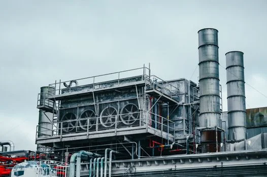
Technology selection for a semiconductor fab requires weighing each method's capabilities, limitations, and suitability against contaminant profile and reuse goals. The following comparison table outlines the key performance metrics and use cases for leading technologies:
| Technology | Contaminant Removal (COD/TSS/Metals) | Water Reuse Rate (%) | CapEx (¥/m³/h) | OPEX (¥/m³) | Footprint (m²/100 m³/h) | Membrane Lifespan (years) | Best For |
|---|---|---|---|---|---|---|---|
| Reverse Osmosis (RO) | 99%+ COD, 99%+ TSS, 99%+ Dissolved Salts | 80–95% | 1.2M–8M (for 10–100 m³/h) | 10–25 | ~50 | 3–5 (with proper pretreatment) | High-purity water production, general contaminant removal. |
| MBR (Membrane Bioreactor) | 95%+ COD, 99.9% TSS, 90%+ Metals (pre-treatment dependent) | 70–90% (as tertiary treatment) | 1.5M–10M (for 10–100 m³/h) | 8–18 | ~30 (60% smaller than conventional) | 10+ (for membranes) | High-TOC streams (photoresist), space-constrained fabs. |
| Ion Exchange | Selective for specific ions (e.g., metals, hardness) | N/A (polishing step) | 0.5M–3M (for 10–100 m³/h) | 15–30 (resin regeneration) | ~20 | N/A (resin lifespan) | Targeted removal of specific dissolved contaminants. |
| Chemical Precipitation | Moderate COD, High TSS, Moderate Metals | N/A (pre-treatment) | 0.3M–1.5M (for 10–100 m³/h) | 5–15 (chemical costs) | ~40 | N/A | Initial removal of HF, metals, and suspended solids. |
| Integrated RO+MBR | 99.9%+ COD, 99.9%+ TSS, 99%+ Metals | 95%+ | 2M–15M (for 10–100 m³/h) | 12–22 | ~40 | 3–5 (RO), 10+ (MBR) | Achieving ZLD, maximum water reuse. |
Reverse Osmosis (RO) systems excel at removing dissolved salts, COD, and TSS, achieving 99%+ removal rates and enabling 80–95% water reuse. Spiral-wound elements cannot be backpulsed, so accumulated foulants show up directly as capacity loss (Wikipedia, Reverse osmosis). Typical CapEx for industrial RO systems for wafer fab wastewater treatment ranges from ¥1.2M–¥8M for 10–100 m³/h capacity.
MBR (Membrane Bioreactor) systems are highly effective for high-TOC streams, such as those from photoresist processes, achieving over 99.9% TMAH removal and offering a significantly smaller footprint (60% smaller than conventional systems). MBR membranes have a lifespan of 10+ years. Ion exchange is best suited for selective removal of specific ions like copper and cobalt, often used as a polishing step, but is limited for high-TOC streams and requires resin regeneration. Chemical precipitation is effective for initial removal of HF and metals but generates sludge that requires disposal, often necessitating solutions like filter presses. An integrated RO+MBR approach offers the highest water reuse rates (95%+) and contaminant removal, approaching zero-liquid-discharge (ZLD) goals.
Zero-Fouling Design Strategies for Wafer Fab Treatment Equipment
Zero-fouling RO pretreatment for semiconductor wastewater rests on three levers: robust pretreatment, optimized chemical dosing, and disciplined membrane operation. Skip any one of them and a 3–5 year membrane budget turns into an annual one. The subsections below map each lever to equipment and setpoints.
Silica Antiscalant Dosing for Semiconductor RO System: Getting the Number Right
Silica antiscalant dosing for semiconductor RO system feeds is calibrated from water chemistry and flow rate, never from a brochure value. Antiscalants disperse colloids and metal oxides and control carbonate, phosphate, sulfate, and fluoride scales at a fraction of the acid dose needed for equivalent protection (Wikipedia, Reverse osmosis). automated antiscalant dosing systems hold that dose steady against the pH 2–12 swings of tool dumps. Field practice we apply: lock the dose during the commissioning test window, then re-verify after every fab process change.
For RO feed conditioning, comprehensive pretreatment is non-negotiable. multi-media filters strip suspended solids (TSS) that would clog elements within days. Cartridge filtration at 1–5 µm and pH adjustment complete the standard train, with acid dosing keeping carbonates in soluble form (Wikipedia, Reverse osmosis). These measures are integral to the zero-fouling design strategies for RO membranes in semiconductor applications we specify for etching drains.
MBR systems mitigate fouling through inherent design features and operational protocols. Submerged PVDF membranes, such as those in MBR membrane bioreactor modules, are equipped with integrated aeration systems that support biology while scouring the membrane surface. Automated backwash cycles add a second cleaning layer. Advanced MBR designs, like those discussed in MBR systems for high-TOC semiconductor wastewater streams, are engineered for continuous operation with minimal fouling.
Common fouling symptoms include a steady increase in transmembrane pressure (TMP), reduced water flux, and increased energy consumption. Diagnostic steps for identifying fouling culprits involve detailed influent characterization (TOC, silica, specific metals analysis), membrane autopsy to examine deposited materials, and analysis of backwash water. A robust zero-fouling checklist for operational reliability should include:
- 1. Comprehensive Influent Characterization: Detailed analysis of TOC, silica, metals, pH, and TSS from each wastewater stream.
- 2. Optimized Pretreatment Selection: Ensuring appropriate filtration (e.g., multi-media, ultrafiltration) and chemical pretreatment (e.g., coagulation, pH adjustment) are in place.
- 3. Antiscalant Dosing Optimization: Calibrating antiscalant dosage based on water chemistry and flow rates to prevent silica and mineral scaling.
- 4. Effective Membrane Cleaning Protocols: Establishing regular Clean-In-Place (CIP) frequencies and using validated cleaning chemicals tailored to identified foulants.
Step-by-Step Selection Framework for Wafer Fab Wastewater Treatment Equipment
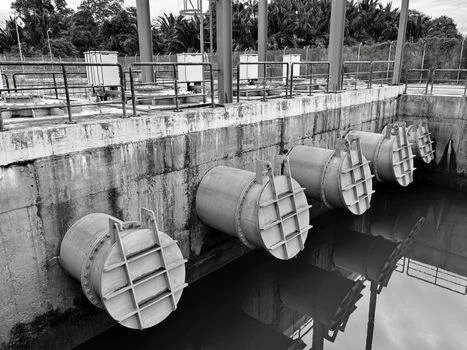
Equipment selection for wafer fab effluent impacts operational costs, compliance, and water security for the life of the plant. A structured approach minimizes procurement risk and ensures the chosen system meets the fab's unique demands. Follow these steps for a robust selection process:
- Define Objectives and Regulatory Requirements: Clearly articulate the primary goals: meeting SEMI S23 discharge limits, achieving high-percentage water reuse (e.g., 80–95%), or pursuing Zero Liquid Discharge (ZLD). Identify all applicable local, national, and international regulations.
- Characterize Wastewater Streams: Conduct thorough laboratory analysis of each distinct wastewater stream (SC1/SC2, CMP, photoresist, etching). Key parameters to measure include TOC, silica, aluminum, copper, cobalt, HF, TSS, pH, and conductivity. Accurate characterization is foundational for technology selection.
- Match Technology to Contaminant Profile: Utilize the technology comparison table provided earlier. For high-TOC streams, MBR systems are often preferred. For high-silica and dissolved solids, RO with advanced pretreatment is essential. Ion exchange can be a valuable polishing step for specific metal removal. Integrated RO+MBR systems are typically required for ZLD goals.
- Size the System and Estimate Costs: Determine the required treatment capacity (e.g., 10–100 m³/h) based on current and projected fab throughput. Consider the CapEx range (¥1.2M–¥8M for 10–100 m³/h RO systems) and estimate OPEX, including energy consumption (0.5–1.5 kWh/m³), chemical consumption, and membrane replacement costs. Refer to Wafer Cleaning Wastewater Treatment by Reverse Osmosis: 2026 Engineering Specs for detailed cost benchmarks.
-
Evaluate Vendors Using a Comprehensive Checklist: Beyond technical specifications, assess vendors based on:
- Proven experience in semiconductor wastewater treatment.
- Demonstrated success in zero-fouling design and membrane longevity.
- Ability to meet SEMI S23 and other relevant compliance standards.
- Transparency in CapEx and OPEX projections, including lifecycle costs.
- Robust after-sales support, including spare parts, technical assistance, and training for membrane replacement and CIP procedures.
One siting note for compounds short on land: sanitary drains from fab offices and canteens can run through an Underground Package Sewage Treatment Plant (WSZ Series), keeping domestic sewage separate from process effluent and freeing surface area for the process train.
Semiconductor Wastewater Reuse System CapEx OPEX Comparison
Advanced wafer fab treatment equipment pays back through water reuse, regulatory compliance, and operational efficiency. A detailed cost-benefit analysis is crucial for stakeholder buy-in. The cost breakdown for a typical 50 m³/h system can be substantial, but the savings often outweigh the initial investment—consider these cost categories:
| Cost Category | CapEx (¥) | OPEX (¥/year) | Notes |
|---|---|---|---|
| Equipment (e.g., RO/MBR) | 4M–6M | - | Based on 50 m³/h capacity. |
| Pretreatment (Multi-media Filter, Dosing Systems) | 0.5M–1M | ~50K–100K | Includes media replacement, chemical tanks. |
| Installation & Commissioning | 1M–2M | - | Varies by site complexity. |
| Membrane Replacement (RO) | - | 500K–1M | Every 3–5 years; accounts for fouling. |
| Energy Consumption (0.5–1.5 kWh/m³) | - | ~300K–900K | At 8,760 hours/year operation. |
| Chemicals (Antiscalant, CIP) | - | 100K–300K | Depends on water chemistry. |
| Labor (Operation & Maintenance) | - | 200K–400K | Dedicated operator/technician. |
| Sludge Disposal (if applicable) | - | 50K–150K | From precipitation/filtration steps. |
| Total Estimated Annual OPEX | ~1.15M–2.85M |
The ROI calculation for a 50 m³/h system operating at 90% reuse can be compelling. Assuming a freshwater cost of ¥50/m³, annual water savings alone could reach ¥3 million (50 m³/h × 24 h/day × 365 days/year × 0.90 reuse × ¥50/m³). Avoiding regulatory fines, which can amount to ¥5 million annually for non-compliance, adds significant value. For a large-scale fab, the reduction in freshwater withdrawal can translate to savings upwards of ¥12 million per year, as seen in the TSMC Arizona example. Exploring financing options such as leasing or leveraging government incentives for water reuse projects can further improve financial viability.
Reuse can also feed ultrapure production directly: some fabs now route reclaimed wastewater into UPW plants, using UV advanced oxidation to strip stubborn organics such as urea for sub-7 nm fabrication (Wikipedia, Ultrapure water). That loop—effluent to RO-grade reuse to UPW feedstock—is where the savings above compound year over year.
Who This Is For / Next Step
Process engineers, EPC utilities leads, and procurement teams specifying treatment for fabs at 10–100+ m³/h are the audience for this guide. Sites without CMP, photoresist, or HF loads—LED packaging or back-end assembly—will find simpler trains sufficient. If you have stream assay data and a target reuse percentage, send them through our process design inquiry form so a process engineer can map pretreatment, CapEx band, and membrane budget before tender.

Frequently Asked Questions
What is the biggest challenge in treating wafer fab wastewater?
Membrane fouling from photoresist residues and silica scaling is the primary challenge, capable of cutting RO membrane lifespan by 30–50% without proper pretreatment and antiscalant dosing. TOC at 500–2,000 mg/L coats elements, while silica at 100–300 mg/L scales surfaces. Zero-fouling design—filtration, dosing, and CIP discipline—is the countermeasure that keeps reuse on target.
How much does wafer fab wastewater treatment equipment cost?
CapEx for wafer fab treatment equipment ranges from ¥1.2M for a 10 m³/h RO system to ¥20M+ for a 100 m³/h zero-liquid-discharge train. OPEX is dominated by membrane replacement at ¥500K–¥2M/year and energy at 0.5–1.5 kWh/m³. A 50 m³/h integrated system typically lands near ¥5.5M–¥9M installed, based on the cost table above.
Can MBR systems handle high-TOC wastewater from photoresist streams?
Yes, MBR systems are well suited to high-TOC photoresist streams, achieving 99.9% TOC removal with submerged PVDF membranes and integrated aeration scour. Their footprint runs about 60% smaller than conventional biology, and membrane life can exceed 10 years. For TMAH-bearing etch drains, see MBR systems for high-TOC semiconductor wastewater streams.
What is the SEMI S23 compliance reverse osmosis reuse rate?
RO-based reuse trains typically deliver 80–95% water recovery against SEMI S23-linked discharge targets of COD below 50 mg/L and TSS below 10 mg/L. The EU Industrial Emissions Directive, revised as Directive 2024/1785 in force August 2024, and China's Water Ten Plan push 70%+ water reuse by 2035. Compliance margin, not the recovery headline, usually decides the final design.
How often do RO membranes need to be replaced in wafer fab applications?
RO membranes in wafer fab duty are typically replaced every 3–5 years. Silica scaling and photoresist residues can cut that lifespan by 30–50% when fouling prevention lapses; see zero-fouling design strategies for RO membranes in semiconductor applications. Disciplined antiscalant dosing and scheduled CIP keep replacement on the budgeted cycle.
Related Equipment
- MBR systems for high-TOC wafer fab wastewater streams — view specifications, capacity range, and technical data
Need a customized solution? Request a free quote with your specific flow rate and pollutant parameters.