Chip fab wastewater treatment in 2026 requires specialized systems to handle high variability (pH 2–12), zero-nutrient streams (BOD <50 mg/L), and contaminants like TMAH (10–100 mg/L) and fluoride (50–300 mg/L). A typical 5 MGD fab needs a multi-stage system: dissolved air flotation (DAF) for 95%+ TSS removal, membrane bioreactors (MBR) for biological treatment (0.1 μm filtration), and reverse osmosis (RO) for 90% water recovery. CAPEX ranges from $5M–$50M, with CHIPS Act-funded projects requiring EPA NPDES compliance and local water reuse targets.
Why Chip Fab Wastewater Defeats Conventional Treatment Systems
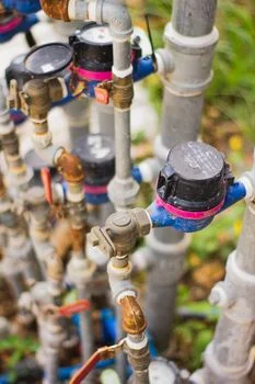
Advanced node semiconductor manufacturing generates wastewater with pH fluctuations from 2.0 to 12.0 and silica concentrations exceeding 200 mg/L, exceeding the treatment capacity of standard industrial systems. Conventional wastewater plants are designed for steady-state organic loads, but a chip fab wastewater treatment company must account for the rapid transition between hydrofluoric acid (HF) etching cycles and alkaline cleaning steps. These swings can occur within 60 to 120 minutes, requiring automated chemical dosing systems capable of delivering sulfuric acid or caustic soda at rates of 0.5–2 L/min to maintain a stable influent pH for downstream biological processes.
The organic profile of fab effluent is dominated by Tetramethylammonium Hydroxide (TMAH), a developer that is both toxic to standard nitrifying bacteria and highly resistant to simple aeration. many fab streams are "zero-nutrient," with Biochemical Oxygen Demand (BOD) often falling below 50 mg/L. This lack of carbon starves biological systems, leading to biomass washout unless specialized MBR designs are employed with external carbon dosing, such as methanol or acetic acid at 5–10 mg/L. Without these modifications, the biological system fails to maintain the Mixed Liquor Suspended Solids (MLSS) levels necessary for contaminant degradation.
Flow rate fluctuations also pose a significant risk to system stability. Tool sets for 3nm and 2nm nodes can discharge between 50 and 500 GPM depending on the batch cleaning cycle. A real-world example of this challenge occurred at a Tier-1 fab where untreated Chemical Mechanical Planarization (CMP) slurry—rich in abrasive silica nanoparticles—bypassed a poorly calibrated pretreatment stage and fouled a Dissolved Air Flotation (DAF) system within four hours, forcing a total fab shutdown. Effective treatment requires robust equalization and specific pretreatment for high-solids streams.
| Contaminant | Typical Influent Range | Treatment Challenge | Target Effluent (2026) |
|---|---|---|---|
| TMAH | 10–100 mg/L | Toxicity to bacteria; high COD | <0.1 mg/L |
| Fluoride | 50–300 mg/L | Scaling; EPA discharge limits | <4.0 mg/L |
| Silica (SiO2) | 50–200 mg/L | Severe membrane fouling/scaling | <10 mg/L (pre-RO) |
| BOD | <50 mg/L | Nutrient starvation for biology | N/A (requires dosing) |
| Copper/Nickel | 1–10 mg/L | Heavy metal toxicity | <0.05 mg/L |
Process Flow for Chip Fab Wastewater Treatment: From Pretreatment to ZLD
A 5 MGD semiconductor fab requires a four-stage treatment architecture to ensure zero-fouling operation and compliance with 2026 environmental standards. The process begins with Stage 1: Pretreatment, where a high-efficiency DAF system for TSS removal in semiconductor fabs targets the CMP slurry and abrasive particles. By dosing Polyaluminum Chloride (PAC) at 10–30 mg/L and polymer at 1–3 mg/L, the DAF achieves 95%+ TSS removal efficiency, protecting downstream membranes from physical abrasion.
Stage 2: Biological Treatment utilizes a zero-fouling MBR system for TMAH and COD removal in semiconductor fabs. This stage is critical for breaking down complex organics. The MBR operates with 0.1 μm PVDF membranes and maintains an MLSS concentration of 8,000–12,000 mg/L. To handle the unique chemistry of 3nm node waste, the system requires an aeration rate of 0.2–0.4 m³/m²·h to ensure complete nitrification and TMAH oxidation. This is where how MBR systems remove 99.9% of TMAH from etching wastewater becomes the primary mechanism for meeting discharge permits.
Stage 3: Membrane Filtration involves a high-recovery RO system for water reclamation in semiconductor fabs. For standard rinse water, recovery rates reach 90%, but in high-silica streams, this may drop to 70% to prevent irreversible scaling. The RO stage uses spiral-wound polyamide membranes operating at 8–12 bar, supported by antiscalant dosing at 5–10 mg/L. Finally, Stage 4: Zero-Liquid Discharge (ZLD) is employed for brine management. This optional stage uses multi-effect evaporation or crystallization to convert liquid waste into solid salt cake, though it increases energy consumption by 20–30 kWh/m³ and adds approximately 30–50% to the total CAPEX.
| Process Stage | Key Equipment | Critical Parameter | Chemical Dosing |
|---|---|---|---|
| Pretreatment | DAF + Equalization | TSS <20 mg/L | PAC (20 mg/L), Polymer (2 mg/L) |
| Biological | MBR (PVDF) | MLSS: 10,000 mg/L | Methanol (C-Source): 8 mg/L |
| Desalination | High-Pressure RO | 90% Flux Recovery | Antiscalant: 7 mg/L |
| ZLD | Crystallizer | Zero liquid discharge | De-foamer: 0.5 mg/L |
Technology Comparison: MBR vs. RO vs. Ion Exchange vs. Electro-Ceramic Desalination for Fab Streams
Selection of wastewater treatment technology for 3nm/2nm fabs depends on the specific chemical profile of the process stream, as no single technology is optimal for all effluents. MBR is the industry standard for mixed streams containing both organics (TMAH) and solids (CMP slurry), offering 99.9% TMAH removal. However, for high-purity reclaim, such as Ultrapure Water (UPW) recycling, Ion Exchange (IX) is often preferred due to its ability to target specific ionic contaminants at low concentrations, despite the higher OPEX associated with resin regeneration.
Emerging technologies like electro-ceramic desalination are gaining traction for brine management because they can handle higher TDS levels than traditional RO without the same scaling risks. When evaluating RO design specs for treating wafer cleaning wastewater in semiconductor fabs, engineers must weigh the lower CAPEX of RO against the superior fouling resistance of ceramic-based systems. The following matrix provides a technical baseline for procurement teams comparing these four primary technologies.
| Technology | Best For (Stream) | TMAH Removal | Fluoride Removal | CAPEX ($/GPM) | OPEX ($/m³) |
|---|---|---|---|---|---|
| MBR | Mixed Etching/CMP | 99.9% | 80–90% | $2,500–$4,000 | $0.50–$1.00 |
| RO | Wafer Rinse | 95% | 99% | $3,000–$5,000 | $0.80–$1.50 |
| Ion Exchange | UPW Reclaim | 99% | 95% | $1,500–$3,000 | $1.00–$2.00 |
| Electro-Ceramic | Brine/ZLD | 95% | 90% | $4,000–$6,000 | $0.30–$0.60 |
CAPEX and OPEX Benchmarks for Chip Fab Wastewater Systems (2026)
CAPEX for semiconductor wastewater treatment systems in 2026 scales from $5 million for 1 MGD facilities to over $50 million for 10 MGD mega-fabs, driven largely by the degree of automation and ZLD requirements. For a standard 5 MGD project, the equipment typically accounts for 30% of the budget, while installation and specialized piping (often requiring high-purity PVDF or stainless steel) account for another 20%. Automation and continuous monitoring sensors—essential for 3nm node fabs—represent roughly 15% of the total investment. (Zhongsheng field data, 2025).
OPEX is primarily driven by energy consumption (40%) and chemical dosing (25%). MBR systems are relatively energy-efficient at 0.10–0.15 kWh/m³, whereas RO systems require 0.8–1.2 kWh/m³ to overcome osmotic pressure in high-TDS streams. The ROI for water reuse is increasingly favorable as municipal water costs rise. For example, a 5 MGD fab recycling 90% of its water can save over $3 million annually in water procurement and discharge fees, leading to a payback period of approximately 3.5 to 4.5 years. Hidden costs, such as membrane replacement every 3–5 years for RO ($50–$100/m²), must be factored into long-term budget planning.
| Fab Size (Flow) | Estimated CAPEX | Annual OPEX | Energy (kWh/m³) |
|---|---|---|---|
| 1 MGD | $5M – $10M | $0.6M – $1.2M | 0.4 – 0.6 |
| 5 MGD | $12M – $25M | $2.8M – $5.5M | 0.5 – 0.8 |
| 10 MGD | $25M – $50M | $6.0M – $11.0M | 0.6 – 1.0 |
CHIPS Act Compliance: Wastewater Treatment Requirements for Semiconductor Fabs
CHIPS Act funding for new semiconductor facilities is contingent upon meeting a 50% minimum water reuse threshold and strict EPA NPDES discharge limits. These regulations are designed to minimize the impact of "water-stressed" regions, such as Arizona and Texas, where many new 2nm fabs are located. To qualify for the 10–20% additional funding incentives available for sustainable infrastructure, fabs must often implement ZLD systems for brine management in semiconductor fabs, ensuring that no liquid waste leaves the site boundary.
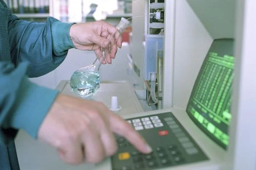
Compliance also dictates continuous monitoring and reporting of specific toxic contaminants. The EPA NPDES 2024 limits for semiconductor discharge are significantly more stringent than general industrial standards, particularly for TMAH (1.5 mg/L) and Fluoride (4.0 mg/L). Automated sampling systems, including online TOC (Total Organic Carbon) analyzers and flow-proportional composite samplers, are now mandatory for CHIPS Act-funded projects to provide a verifiable audit trail of effluent quality. Facilities that fail to meet these targets risk the clawback of federal subsidies and significant local fines.
| Parameter | EPA NPDES Limit | MBR/RO Performance | Compliance Margin |
|---|---|---|---|
| TMAH | 1.5 mg/L | 0.1 mg/L | 93% |
| Fluoride | 4.0 mg/L | 0.5 mg/L | 87% |
| Copper | 0.05 mg/L | 0.01 mg/L | 80% |
| Nickel | 0.1 mg/L | 0.02 mg/L | 80% |
Case Study: Zero-Fouling MBR/RO System for a 3nm Fab in Arizona
A 3nm semiconductor facility in Arizona achieved 85% water reclamation by implementing a zero-fouling MBR/RO integrated system. The fab, processing 5 MGD, faced significant challenges with high-silica wastewater (150–200 mg/L) that caused frequent downtime in its initial pilot system. The final engineering solution involved an optimized DAF pretreatment stage with a 30% higher PAC dose than standard industrial applications to ensure the complete removal of CMP slurry before the water reached the biological tanks.
The system design followed a DAF → Equalization → MBR → RO → ZLD sequence. By maintaining a strict lime softening regimen (200 mg/L dose) prior to the RO stage, the facility successfully mitigated silica scaling, allowing the RO units to maintain a 90% recovery rate. Post-treatment data confirmed effluent quality of TMAH <0.1 mg/L and Fluoride <1 mg/L, well within EPA limits. The total CAPEX for the project was $22M, with an OPEX of $1.20/m³. Given the high cost of municipal water in the desert region ($2.50/m³), the facility realized a 4.2-year payback period, demonstrating that advanced wastewater treatment is a financial asset as much as a compliance necessity.
Frequently Asked Questions
Q: What is the biggest challenge in treating chip fab wastewater?
A: The zero-nutrient streams (BOD <50 mg/L) starve biological systems, requiring external carbon dosing (e.g., methanol at 5–10 mg/L) and specialized MBR designs with longer retention times (12–24 hours) to effectively degrade TMAH.
Q: How much does a chip fab wastewater treatment system cost?
A: CAPEX ranges from $5M–$50M for a 1–10 MGD fab, with ZLD systems adding 30–50%. OPEX is $0.50–$1.50/m³, driven by energy (40%) and membrane replacement (15%).
Q: Can reverse osmosis (RO) treat chip fab wastewater?
A: Yes, but silica scaling reduces recovery to 70% without pretreatment like lime softening. RO achieves 99% fluoride removal and 95% TMAH removal, but MBR is superior for high-organic mixed streams.
Q: What are the EPA limits for chip fab wastewater discharge?
A: According to 2024 NPDES guidelines, limits include TMAH at 1.5 mg/L, fluoride at 4 mg/L, copper at 0.05 mg/L, and nickel at 0.1 mg/L. MBR systems typically achieve TMAH <0.1 mg/L.
Q: How does the CHIPS Act affect wastewater treatment for fabs?
A: Funded projects must recycle at least 50% of wastewater and meet strict EPA discharge permits. Achieving Zero-Liquid Discharge (ZLD) can qualify a project for 10–20% in additional federal funding.