Wafer cleaning wastewater treatment by reverse osmosis (RO) achieves 99%+ removal of dissolved salts, TOC, and metals (e.g., aluminum <3 mg/L, sodium <150 mg/L) while enabling 80–95% water reuse in semiconductor fabs. However, organic fouling from photoresist residues and silica scaling reduces membrane lifespan by 30–50% without pretreatment. This guide provides 2026 engineering specs, zero-fouling design strategies, and CapEx benchmarks (¥1.2M–¥8M for 10–100 m³/h systems) to meet SEMI S23 and local discharge limits.
Why Wafer Cleaning Wastewater Demands Reverse Osmosis: Contaminant Profiles & Fab Challenges
Wafer cleaning wastewater contains high levels of Total Organic Carbon (TOC) ranging from 500–2,000 mg/L primarily from photoresist residues, alongside silica concentrations of 100–300 mg/L and trace metals such as aluminum, copper, and cobalt at 5–50 mg/L. Unlike municipal wastewater, semiconductor effluent is characterized by extreme pH swings and the presence of complexing agents that make traditional precipitation methods insufficient. Reverse osmosis is uniquely suited for this application because it provides a physical barrier capable of rejecting both ionic species and non-biodegradable organic molecules that would otherwise pass through biological systems.
In a modern fab, wastewater is typically segregated into three primary streams. The first is the SC1/SC2 cleaning stream, which is rich in ammonia and hydrogen peroxide. The second is Chemical Mechanical Planarization (CMP) wastewater, which contains high concentrations of colloidal silica and metal interconnect materials. The third is photoresist stripping wastewater, which carries the highest organic load in the form of solvents like PGMEA and TMAH. Conventional biological treatment often fails in these environments because high salinity inhibits microbial growth, and heavy metals can poison the biomass, leading to system instability (Zhongsheng field data, 2025).
| Parameter | SC1/SC2 Cleaning | CMP Wastewater | Photoresist Stripping |
|---|---|---|---|
| pH Range | 2.0 – 11.0 | 6.5 – 9.0 | 8.0 – 12.0 |
| TOC (mg/L) | 50 – 200 | 100 – 400 | 500 – 2,000 |
| Silica (mg/L) | <10 | 150 – 500 | <20 |
| Total Dissolved Solids (mg/L) | 500 – 1,500 | 300 – 800 | 1,000 – 3,500 |
| Key Metals | Al, Fe | Cu, Co, Ru | Trace metals |
The financial imperative for water reuse is driven by the rising cost of Ultrapure Water (UPW). Producing UPW for 5nm+ nodes costs approximately $2–$5/m³ when accounting for energy, chemicals, and resin replacement. By implementing high-recovery RO systems, fabs can recycle up to 95% of their cleaning water, significantly reducing the demand for fresh intake and lowering the burden on local municipal utilities.
Reverse Osmosis for Wafer Cleaning Wastewater: Process Flow & Membrane Selection
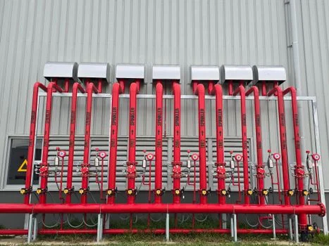
A standard 2-stage RO configuration for semiconductor applications requires a multi-step pretreatment sequence to ensure the Silt Density Index (SDI) remains below 3.0 before entering the membrane skids. The process begins with pH adjustment to 6.5–7.5 to stabilize silica and prevent premature scaling. For streams with Total Suspended Solids (TSS) exceeding 500 mg/L, such as CMP wastewater, DAF systems for TSS and photoresist removal in semiconductor wastewater are deployed to remove light organic flocs and colloidal particles that would otherwise clog the RO feed spacers.
Following primary clarification, the water passes through multimedia filtration and, in some cases, ultrafiltration (UF) to remove particles down to 0.01 μm. The RO stage itself is typically a 2-stage design: the first stage achieves approximately 75% recovery, and the second stage treats the concentrate of the first to push total system recovery above 90%. For 5nm nodes, a final polishing step using Ion Exchange (IX) is often required to reach the ultra-low metal limits specified by SEMI S23.
| Membrane Type | Material | Flux (LMH) | Salt Rejection (%) | pH Tolerance |
|---|---|---|---|---|
| High-Rejection Polyamide | Thin-film Composite | 15 – 25 | 99.7% | 2 – 11 |
| Fouling-Resistant (FR) | Modified Polyamide | 12 – 20 | 99.5% | 3 – 10 |
| Low-Pressure (LP) | Polyamide | 20 – 30 | 99.0% | 4 – 10 |
Chemical conditioning is critical for managing the high silica loads found in wafer cleaning. Using precision antiscalant and cleaning chemical dosing for RO systems, engineers apply silica inhibitors like polyacrylic acid at rates of 2–5 mg/L. This dosing prevents the formation of hard silica scale on the membrane surface, which is notoriously difficult to remove once established. The 2-stage RO approach is essential for meeting the <50 ppb TOC requirement of SEMI S23, as the second stage acts as a high-efficiency polisher for small organic molecules that might bypass the first stage.
Fouling Prevention in Semiconductor RO Systems: Design Strategies & Cleaning Protocols
Organic fouling from photoresist residues represents the primary cause of flux decline in semiconductor RO systems, often resulting in a 30% increase in feed pressure within the first month of operation if not properly managed. Photoresist polymers are hydrophobic and tend to adsorb onto the polyamide surface of standard RO membranes. To combat this, zero-fouling design strategies prioritize the removal of these organics before they reach the high-pressure pumps.
When TOC levels exceed 1,000 mg/L, DAF is the preferred pretreatment as it can remove 70–90% of photoresist residues through air-assisted flotation. For lower TOC concentrations (<500 mg/L), activated carbon or precoat filtration may be used. If fouling does occur, a structured Clean-In-Place (CIP) protocol must be followed. Monitoring the Normalized Permeate Flow (NPF) is the most effective way to trigger cleaning; a decline of >10% in NPF or an increase of >1.5 bar in differential pressure indicates that a CIP cycle is necessary.
| Foulant Type | Cleaning Chemical | Concentration | Temperature/Time |
|---|---|---|---|
| Organic (Photoresist) | NaOH (Sodium Hydroxide) | 0.1% (pH 11-12) | 35°C / 60 min |
| Inorganic Scale (Silica) | Ammonium Bifluoride | 0.5 – 1.0% | 30°C / 45 min |
| Metals/Carbonates | Citric Acid | 2.0% (pH 2-3) | 40°C / 30 min |
Advanced diagnostic techniques such as membrane autopsies using Scanning Electron Microscopy (SEM) and Energy Dispersive X-ray (EDX) allow fab managers to identify the exact elemental composition of foulants. This data is used to refine the pretreatment chemistry, potentially adjusting the coagulant type or the antiscalant blend to match the specific wastewater profile of the production line.
Effluent Quality & Compliance: Meeting SEMI S23, EPA, and Local Discharge Limits
Compliance for 5nm+ semiconductor nodes is governed by the SEMI S23 standard, which sets rigorous targets for water and energy efficiency. To meet these standards for wafer cleaning reuse, the RO effluent must achieve TOC levels below 50 ppb and metal concentrations (such as copper, cobalt, and ruthenium) below 1 ppb. While RO is highly effective at removing bulk contaminants, reaching these ultra-low levels often requires the integration of chelating agents to break down metal-EDTA complexes and IX polishing to capture residual ions.
Regional discharge limits also play a significant role in system design. In semiconductor hubs like Singapore or Taiwan, local regulations often stipulate Ammonia-Nitrogen levels below 10 mg/L and Chemical Oxygen Demand (COD) below 200 mg/L for discharge into public sewers. Achieving these targets requires a robust RO system that can handle the high rejection of nitrogenous compounds found in SC1 cleaning solutions.
| Parameter | SEMI S23 (Reuse) | Taiwan (Discharge) | Arizona, USA (Discharge) |
|---|---|---|---|
| TOC / COD | <50 ppb (TOC) | <100 mg/L (COD) | <200 mg/L (COD) |
| Total Metals | <1 ppb | <1.0 mg/L | <2.0 mg/L |
| Silica | <10 ppb | N/A | N/A |
| Ammonia-N | <100 ppb | <15 mg/L | <25 mg/L |
Online monitoring is indispensable for maintaining compliance. High-precision TOC analyzers, such as the Sievers 500 RL, provide real-time data on organic breakthrough, while conductivity meters monitor the salt rejection performance of each RO stage. Particle counters are also deployed post-RO to ensure that no colloidal silica or membrane fragments are entering the UPW makeup loop.
Cost Analysis: CapEx, OPEX, and ROI for Semiconductor RO Systems
The investment in a semiconductor-grade RO system is significant, with CapEx ranging from ¥1.2M for small 10 m³/h pilot systems to over ¥8M for large-scale 100 m³/h installations. This cost includes the RO skids, high-pressure pumps, pretreatment filtration, and the necessary automation for chemical dosing. For a typical 50 m³/h system, the RO skid itself accounts for approximately 50% of the total investment, with pretreatment and IX polishing making up the remainder.
OPEX is dominated by energy consumption and membrane replacement costs. Modern energy-efficient RO designs for high-salinity wastewater utilize energy recovery devices (ERDs) to reduce power consumption to 0.8–1.2 kWh/m³. Chemical costs for antiscalants and CIP agents typically range from ¥0.2–¥0.5/m³ of treated water. Despite these costs, the ROI is often achieved within 2 to 4 years due to the massive savings in UPW procurement and the avoidance of heavy discharge tariffs in water-stressed regions.
| Technology | CapEx (50 m³/h) | OPEX (per m³) | TOC Removal | Water Reuse? |
|---|---|---|---|---|
| Reverse Osmosis (RO) | ¥4M – ¥6M | ¥1.5 – ¥2.5 | 99%+ | Yes (80-95%) |
| MBR (Biological) | ¥2M – ¥3.5M | ¥0.8 – ¥1.5 | 70-85% | Partial |
| Evaporation (MVR) | ¥10M – ¥15M | ¥15 – ¥30 | 99.9% | Yes (ZLD) |
In regions like Singapore, where the water tariff can exceed $2.74/m³, the payback period for a 50 m³/h RO system can be as short as 24 months. by reducing the volume of wastewater discharged, fabs minimize their exposure to environmental fines and regulatory risks associated with local water scarcity.
RO vs. MBR vs. Evaporation: Which Technology is Right for Your Fab?
Choosing the right technology depends on the fab's specific goals for water reuse versus simple discharge compliance. Reverse Osmosis is the gold standard for high-quality water reuse because it removes both ions and organics to levels suitable for UPW makeup. However, it is sensitive to fouling. In contrast, MBR systems for semiconductor wastewater with lower TOC residuals offer a lower CapEx and are more resilient to organic fluctuations, but they cannot achieve the ultra-low TOC and salt removal required for 5nm node cleaning processes.
Evaporation technologies like Mechanical Vapor Recompression (MVR) are reserved for Zero Liquid Discharge (ZLD) mandates. While they eliminate the risk of membrane fouling, their energy consumption is 50–100 times higher than RO, and the CapEx is often triple that of a membrane-based system. A decision framework for fab managers usually follows a hierarchy: RO for reuse, MBR for pre-discharge treatment of low-strength streams, and Evaporation only when discharge is strictly prohibited.
| Metric | Reverse Osmosis | MBR | Evaporation |
|---|---|---|---|
| Footprint | Medium | Compact | Large |
| Scalability | High (Modular) | Medium | Low |
| Energy Intensity | Low-Medium | Low | Very High |
| Effluent Quality | Ultra-Pure | Secondary Grade | Distilled Grade |
| Primary Risk | Membrane Fouling | Biomass Poisoning | Corrosion/Scaling |
For most 5nm+ fabs, the optimal strategy is a hybrid approach: using MBR or DAF as a pretreatment stage to protect semiconductor-grade RO systems with 95%+ recovery. This configuration balances capital investment with long-term operational stability and maximum water recovery.
Frequently Asked Questions
Q: How does reverse osmosis handle photoresist stripping solvents like TMAH?A: RO membranes provide high rejection for TMAH (Tetramethylammonium hydroxide) due to its ionic nature in aqueous solutions. However, high concentrations can increase the osmotic pressure and risk organic fouling. Pretreatment with DAF or advanced oxidation is recommended if TMAH concentrations exceed 500 mg/L to protect the RO membranes and ensure permeate quality meets SEMI S23 standards.
Q: Can RO achieve zero liquid discharge (ZLD) for a semiconductor fab?A: RO alone cannot achieve ZLD because it produces a concentrate stream (brine). To reach ZLD, the RO concentrate must be further treated by an evaporator or crystallizer. However, high-recovery RO systems can reduce the volume of wastewater by up to 95%, significantly downsizing the expensive evaporation equipment needed for the final ZLD step.
Q: What is the typical lifespan of an RO membrane in a wafer cleaning application?A: With proper DAF and UF pretreatment, RO membranes in semiconductor applications typically last 2 to 3 years. Without adequate pretreatment, organic fouling from photoresists and silica scaling can reduce this lifespan to less than 12 months. Regular CIP cycles every 3–6 months are essential to maintain flux and rejection performance over the membrane's life.
Q: Does RO remove trace metals like Ruthenium and Cobalt used in 5nm nodes?A: Yes, RO typically removes >99% of these metals. However, because 5nm+ nodes have extremely strict limits (<1 ppb), RO is often followed by a selective Ion Exchange (IX) polishing stage. This "multi-barrier" approach ensures that even trace amounts of exotic metals are removed before the water is reused in the fab's UPW system.