Why Microelectronics Wastewater Requires Specialized Treatment
Microelectronics wastewater treatment in 2025 demands highly specialized solutions to effectively remove contaminants like tetramethylammonium hydroxide (TMAH) and fluoride. These substances pose significant environmental risks even at very low concentrations. Generic industrial wastewater treatment systems often fall short due to the unique, complex pollutant profile characteristic of semiconductor fabrication processes. Hybrid systems, integrating chemical precipitation (achieving 95%+ TMAH removal), advanced membrane filtration (delivering 99.5% fluoride reduction), and Zero Liquid Discharge (ZLD) technologies, are essential for meeting stringent global discharge standards while enabling substantial water reuse—often exceeding 90%. This guide provides critical engineering specifications, detailed process flows, and comprehensive cost data necessary for designing a microelectronics wastewater treatment system tailored to the specific needs of semiconductor fabs.
The microelectronics industry produces wastewater with qualitative contaminants, such as TMAH and ammonium, alongside heavy metals, typically found in low concentrations ranging from 1 to 500 mg/L. Despite these low concentrations, these pollutants exhibit high environmental toxicity, as noted in a 2024 review by Springer. Key pollutants commonly encountered include TMAH (50–200 mg/L), fluoride (10–100 mg/L), arsenic (0.1–5 mg/L), and silica (50–300 mg/L). Each of these requires distinct and often multi-stage treatment methodologies to achieve compliance. Regulatory frameworks such as EPA 40 CFR Part 469 (Semiconductor Manufacturing Effluent Guidelines), the EU Industrial Emissions Directive 2010/75/EU, and China’s GB 31573-2015 set strict microelectronics discharge limits, compelling advanced treatment approaches. For instance, a 2024 wafer fab in Taiwan faced substantial fines totaling $1.2 million due to TMAH exceedances, underscoring the critical need for compliance systems capable of achieving over 99% removal efficiency, as documented in a 2023 case study by Veolia.
| Contaminant | Typical Concentration Range (mg/L) | Primary Source | Environmental/Health Risk | Target Effluent Limit (mg/L) | Required Removal Efficiency |
|---|---|---|---|---|---|
| TMAH | 50–200 | Photoresist developer | Acute toxicity to aquatic life (LC50 = 10–50 mg/L for fish) | < 1.0 (EPA) | >99% |
| Fluoride | 10–100 | Wet etching processes | Skeletal fluorosis (>1.5 mg/L in drinking water) | < 5.0 (WHO/Local) | 90–99.5% |
| Arsenic | 0.1–5 | CMP slurries, plating | Carcinogen, toxic to aquatic life | < 0.1 (EPA) | >95% |
| Copper | 0.5–10 | Plating, etching | Toxic to aquatic life | < 1.3 (EPA) | >90% |
| Nickel | 0.2–8 | Etching, plating | Toxic to aquatic life, potential carcinogen | < 0.2 (EPA) | >90% |
| Silica | 50–300 | Wafer grinding, CMP | RO membrane fouling, scaling | < 10–20 (for RO pretreatment) | >80% (for RO) |
| COD (Organic Solvents) | 500–2,000 | Cleaning, stripping | Oxygen depletion in water bodies | < 100–200 (local limits) | 85–95% |
Contaminant Profile: What’s in Microelectronics Wastewater and Why It Matters
Understanding the precise composition of microelectronics wastewater is paramount for designing an effective treatment system. The industry generates a complex mix of organic and inorganic pollutants, each with specific sources and significant environmental and health risks that dictate treatment priorities. Tetramethylammonium hydroxide (TMAH), widely used as a photoresist developer, is highly toxic to aquatic life, with reported LC50 values for fish in the range of 10–50 mg/L. To meet environmental regulations, treatment processes must achieve a TMAH removal efficiency exceeding 95%, as recommended by EPA 2024 benchmarks.
Fluoride, a common byproduct of wet etching processes, poses a serious public health threat. Ingesting water with fluoride concentrations above 1.5 mg/L can lead to skeletal fluorosis. Semiconductor fabs typically discharge wastewater containing fluoride levels between 10 and 100 mg/L. Effective treatment is therefore essential to reduce this to below 5 mg/L, aligning with World Health Organization (WHO) guidelines. Heavy metals, including arsenic from Chemical Mechanical Polishing (CMP) slurries, copper from plating operations, and nickel from etching baths, are also prevalent. The EPA has established strict discharge limits for these metals: arsenic below 0.1 mg/L, copper below 1.3 mg/L, and nickel below 0.2 mg/L.
Silica, often originating from wafer grinding and CMP processes, presents a significant operational challenge. At concentrations exceeding 50 mg/L, silica can readily foul and scale Reverse Osmosis (RO) membranes, severely reducing their efficiency and lifespan. Consequently, effective pretreatment, such as coagulation and clarification, is crucial to manage silica levels before membrane filtration. the presence of organic solvents like isopropyl alcohol (IPA), acetone, and N-methyl-2-pyrrolidone (NMP) from cleaning steps contributes significantly to the Chemical Oxygen Demand (COD) of the wastewater, often ranging from 500 to 2,000 mg/L. These organic compounds necessitate robust biological or advanced oxidation treatment methods to prevent oxygen depletion in receiving water bodies.
For a detailed guide on addressing TMAH in semiconductor wastewater, consult our comprehensive resource: Semiconductor TMAH Wastewater Treatment: 2025 Engineering Specs, Cost Data & Hybrid Process Design.
Treatment Process Flow: Step-by-Step Engineering for Microelectronics Wastewater
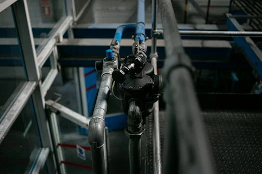
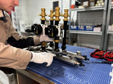
Designing a microelectronics wastewater treatment system involves a carefully sequenced series of steps, often employing a hybrid approach to tackle the diverse contaminant profile. This multi-stage process ensures comprehensive pollutant removal, from gross solids to dissolved contaminants, preparing the water for discharge or reuse. The initial step, pretreatment, is critical for protecting downstream equipment. Mechanical screening, utilizing equipment like the GX Series Rotary Bar Screen, effectively removes large solids (typically those with Total Suspended Solids (TSS) exceeding 500 mg/L), achieving up to 95% TSS removal according to Zhongsheng's 2024 specifications.
Following mechanical screening, chemical precipitation is employed. This stage typically involves dosing lime to raise the pH to between 10 and 11, which is highly effective for fluoride removal, achieving reductions of 90–95%. Simultaneously, coagulants such as ferric chloride are introduced to destabilize and aggregate heavy metal ions. Based on Aries' 2023 data, typical lime dosing rates range from 1.5 to 2.5 kg per cubic meter of wastewater. The resulting flocculated solids are then removed in a primary sedimentation stage. A lamella clarifier, such as the Zhongsheng ZSQ series, is ideal for this purpose, achieving 80–90% TSS removal at surface loading rates of 20–40 m/h.
For facilities with significant organic loads (COD/BOD exceeding 1,000 mg/L), biological treatment becomes a necessary component. An integrated MBR (Membrane Bioreactor) system, like Zhongsheng's DF Series, can effectively reduce these organic parameters by 85–95%. MBR systems utilize membranes with pore sizes typically around 0.1 μm, offering excellent effluent quality and a compact footprint. The subsequent stage involves advanced filtration, primarily using Reverse Osmosis (RO) systems, such as the Zhongsheng Industrial RO System. RO is highly effective for removing residual TMAH and silica, achieving rejection rates exceeding 99%. For microelectronics wastewater, RO recovery rates typically range from 75–85%.
Sludge generated from the sedimentation and precipitation stages requires dewatering to reduce its volume for disposal or potential recycling. A plate and frame filter press, like the Zhongsheng Plate and Frame Filter Press, can reduce sludge volume by approximately 80%, achieving cake solids content of 30–40% according to 2024 specifications. For facilities aiming for complete water recovery and zero discharge, a Zero Liquid Discharge (ZLD) system, involving evaporation and crystallization, is implemented as the final stage. These ZLD systems can achieve 100% water recovery. The capital expenditure (CAPEX) for ZLD systems can range from $3 million to $8 million for a 100 m³/h capacity system, based on 2025 cost data.
| Stage | Equipment Example | Primary Function | Key Performance Indicators | Target Contaminants |
|---|---|---|---|---|
| Pretreatment | Rotary Bar Screen (Zhongsheng GX Series) | Remove coarse solids | 95% TSS removal (for TSS >500 mg/L) | Large debris, rags |
| Chemical Precipitation & Coagulation | Dosing pumps, pH controllers | pH adjustment, heavy metal precipitation, fluoride removal | 90–95% fluoride removal, >90% heavy metal removal | Fluoride, Arsenic, Copper, Nickel |
| Primary Sedimentation | Lamella Clarifier (Zhongsheng ZSQ Series) | Separate suspended solids | 80–90% TSS removal, 20–40 m/h surface loading | Flocculated solids, precipitated metals |
| Biological Treatment (Optional) | MBR System (Zhongsheng DF Series) | Reduce COD/BOD | 85–95% COD/BOD reduction, 0.1 µm membrane pore size | Organic solvents, biodegradable compounds |
| Advanced Filtration | RO System (Zhongsheng Industrial RO) | Remove dissolved solids, TMAH, silica | 99%+ TMAH/silica rejection, 75–85% recovery | TMAH, silica, dissolved salts |
| Sludge Dewatering | Plate and Frame Filter Press (Zhongsheng) | Reduce sludge volume | 80% volume reduction, 30–40% cake solids | Concentrated solids, metals, precipitated compounds |
| ZLD (Optional) | Evaporator & Crystallizer | 100% water recovery, salt production | 95–99% water recovery | All dissolved solids |
Hybrid Treatment Methods: Comparing Chemical, Biological, and Membrane Technologies
Selecting the optimal treatment strategy for microelectronics wastewater involves a careful evaluation of hybrid approaches, balancing cost-effectiveness, removal efficiency, and operational footprint. Chemical precipitation stands out as a cost-effective method for removing fluoride and heavy metals, typically achieving 90–99% removal. However, a significant drawback is the generation of hazardous sludge, which requires specialized handling and disposal. The operational expenditure (OPEX) for chemical precipitation is estimated between $0.50 and $1.50 per cubic meter, based on 2024 OPEX data.
Biological treatment, while highly effective for reducing organic loads like COD and BOD (achieving 85–95% reduction), faces limitations with challenging contaminants such as TMAH, which often requires specifically acclimated biomass. MBR systems, offering a compact footprint of approximately 50–100 m² per 100 m³/h capacity, are increasingly favored for their efficiency and smaller land requirements compared to conventional activated sludge processes.
Membrane filtration, particularly RO and Nanofiltration (NF), offers high removal rates, exceeding 99% for contaminants like TMAH and silica. However, these technologies are susceptible to fouling from dissolved solids and scaling from silica. Effective pretreatment, such as Dissolved Air Flotation (DAF systems), is therefore critical to protect membrane integrity. The OPEX for membrane filtration can range from $1.00 to $3.00 per cubic meter, primarily driven by energy consumption and membrane replacement.
Advanced Oxidation Processes (AOPs), such as ozonation or UV-peroxide systems, are capable of breaking down recalcitrant organic compounds, including TMAH. While these methods can achieve 80–90% TMAH degradation, as reported by Veolia in 2023, they are often energy-intensive and may require careful optimization to manage byproduct formation. A highly effective hybrid approach combines chemical precipitation for initial fluoride and metal removal, followed by an MBR for organic reduction, and finally RO for polishing TMAH and silica. This integrated strategy has demonstrated the capability to achieve 99.5% TMAH removal and facilitate up to 90% water reuse, as validated in a 2024 wafer fab case study.
For more on integrated treatment strategies, explore: Semiconductor Developer Wastewater Treatment: 2025 Engineering Specs, Cost Data & Zero Liquid Discharge Blueprint.
| Technology | Primary Application | Typical Removal Efficiency | Key Advantages | Key Disadvantages | Estimated OPEX ($/m³) | Footprint (Relative) |
|---|---|---|---|---|---|---|
| Chemical Precipitation | Fluoride, Heavy Metals | 90–99% | Cost-effective for high loads, established | Sludge generation, limited organic removal | 0.50–1.50 | Small |
| Biological Treatment (MBR) | COD, BOD | 85–95% | Effective organic removal, compact footprint | Requires acclimated biomass, sensitive to shock loads | 0.75–2.00 | Medium |
| Membrane Filtration (RO/NF) | TMAH, Silica, Dissolved Salts | 99%+ | High purity effluent, high removal rates | Fouling/scaling risk, requires pretreatment, energy-intensive | 1.00–3.00 | Medium |
| Advanced Oxidation (AOP) | Recalcitrant Organics (TMAH) | 80–90% (TMAH degradation) | Breaks down complex molecules | Energy-intensive, potential byproduct formation | 1.50–3.50 | Small to Medium |
| Hybrid (Chem. Precip. + MBR + RO) | Comprehensive (TMAH, F, Metals, Organics) | 99.5%+ (TMAH), 90%+ (Water Reuse) | Addresses diverse contaminants, high reuse | Higher CAPEX, complex operation | 1.50–4.00 | Medium to Large |
Zero-Liquid-Discharge (ZLD) for Microelectronics: Engineering Specs and Cost Breakdown
The implementation of Zero Liquid Discharge (ZLD) systems in microelectronics manufacturing represents the pinnacle of water management, offering complete water recovery and eliminating liquid effluent entirely. A typical ZLD process flow begins with robust pretreatment, followed by RO to remove dissolved solids and challenging contaminants. The concentrated brine from RO then proceeds to an evaporation stage, where water is vaporized, leaving behind highly concentrated salts and solids. Finally, crystallization units solidify these remaining components, resulting in a dry solid waste. This advanced approach achieves exceptional water recovery rates of 95–99%.
The capital expenditure (CAPEX) for ZLD systems in microelectronics applications is substantial, ranging from $3 million to $15 million for systems with capacities between 50 and 200 m³/h, according to 2025 cost data. A typical CAPEX breakdown indicates that approximately 40% is allocated to evaporation equipment, 30% to RO systems, 20% to pretreatment stages, and 10% to crystallization units. Operational expenditure (OPEX) for ZLD is also significant, ranging from $2.50 to $6.00 per cubic meter of treated water. A primary driver of OPEX is energy consumption, with evaporation processes alone requiring 10–15 kWh per cubic meter, as reported by UCC in 2024.
Despite the high initial investment and operating costs, ZLD systems offer compelling return on investment (ROI) drivers. These include substantial savings from reduced freshwater consumption, which can range from $0.50 to $2.00 per cubic meter of water reused. Equally important is the avoidance of significant regulatory fines, which can escalate to $1 million per year for non-compliance. ZLD systems can facilitate byproduct recovery, such as gypsum or even reclaimed TMAH, creating additional revenue streams. A notable case study from 2024 highlighted a fab in Singapore that achieved a 92% reduction in water consumption through ZLD, resulting in annual savings of $1.8 million, according to a 2023 report by Molewater.
| ZLD Component | Typical Capacity Range | Estimated CAPEX Range ($M) | Estimated OPEX Range ($/m³) | Key Benefits | Primary Challenges |
|---|---|---|---|---|---|
| Pretreatment & RO | 50–200 m³/h | 2.0–6.0 | 0.50–1.50 | High purity water, contaminant removal | Fouling, scaling, membrane replacement |
| Evaporation | 50–200 m³/h | 1.5–6.0 | 1.00–3.00 (Energy) | Volume reduction, salt concentration | High energy consumption, scaling potential |
| Crystallization | 50–200 m³/h | 0.5–2.0 | 0.25–0.50 | Solid waste production, further water recovery | Solid handling, waste disposal/recycling |
| Total ZLD System | 50–200 m³/h | 3.0–15.0 | 2.50–6.00 | 100% water recovery, zero discharge, resource recovery | High CAPEX/OPEX, complex operation, energy intensive |
How to Select the Right Microelectronics Wastewater Treatment Equipment
Selecting the optimal microelectronics wastewater treatment equipment requires a systematic approach, ensuring that the chosen solution aligns with specific fab requirements, regulatory mandates, and budgetary constraints. The process begins with a thorough characterization of the wastewater. This involves comprehensive laboratory testing to quantify key contaminants such as TMAH, fluoride, heavy metals, and silica. Utilizing lab-scale jar tests is crucial for determining the precise chemical dosing rates and identifying the most effective coagulants and flocculants, as recommended by Aries' 2023 guidelines. This foundational step ensures that subsequent treatment design is data-driven and efficient.
Next, define clear treatment goals. These typically fall into three categories: meeting stringent discharge limits, achieving high water reuse rates (e.g., 90%+), or implementing a full Zero Liquid Discharge (ZLD) system for 100% water recovery. The chosen goals will significantly influence the complexity and cost of the treatment train. Following goal definition, match the appropriate technologies to the identified contaminants. Referencing comparative tables, such as those detailing the performance of chemical precipitation, biological treatment, and membrane filtration for specific pollutants, is essential. For example, high fluoride concentrations might initially be addressed by chemical precipitation, while TMAH and silica demand advanced membrane filtration.
Equipment sizing is a critical engineering task that depends on the wastewater flow rate (m³/h), influent contaminant concentrations, and the desired effluent quality. For instance, a fab operating at 100 m³/h with an influent TMAH concentration of 100 mg/L would likely require a multi-stage RO system, such as the Zhongsheng 6-RO-100 system, to meet stringent discharge or reuse standards. Budgetary considerations play a significant role, with CAPEX for microelectronics wastewater treatment systems ranging from $1 million to $10 million for capacities between 50 and 500 m³/h. OPEX varies widely, from $0.50/m³ for simpler systems to $6.00/m³ for advanced ZLD configurations, largely dependent on energy consumption and chemical usage.
Finally, vendor selection should prioritize partners with proven experience in the microelectronics sector. Look for manufacturers with a strong track record in designing and implementing specialized systems like MBR systems and RO systems tailored for wafer fabs. A vendor’s ability to provide comprehensive support, from initial design and pilot testing to ongoing operation and maintenance, is invaluable. This structured approach ensures that the selected equipment effectively addresses the unique challenges of microelectronics wastewater treatment, delivering both compliance and operational efficiency.
Frequently Asked Questions
What are the discharge limits for TMAH in microelectronics wastewater?
EPA 40 CFR Part 469 sets a limit of 1 mg/L for TMAH in semiconductor wastewater. The EU’s Industrial Emissions Directive requires stricter limits, often below 0.5 mg/L for new fabs, according to 2024 updates. Local regulations may impose even more stringent requirements.
How much does a microelectronics wastewater treatment system cost?
Capital expenditure (CAPEX) for microelectronics wastewater treatment systems can range from $2.5 million for a 50 m³/h capacity system employing chemical and MBR treatment, up to $15 million for a 200 m³/h Zero Liquid Discharge (ZLD) system, based on 2025 cost data. Operational expenditure (OPEX) typically falls between $0.50 and $6.00 per cubic meter, heavily influenced by the chosen treatment technology, particularly the energy intensity of ZLD systems.
Can microelectronics wastewater be reused in the fab?
Yes, microelectronics wastewater can be effectively reused within the fab with advanced treatment processes, typically involving RO followed by UV disinfection. Reuse rates of 90–95% are achievable, leading to significant reductions in freshwater consumption, often by 50–80%, as demonstrated in numerous 2024 wafer fab case studies.
What are the challenges of treating microelectronics sludge?
Microelectronics sludge presents significant challenges due to its high concentration of hazardous constituents, including heavy metals like arsenic and copper, and residual TMAH. This necessitates specialized sludge stabilization processes before disposal to prevent environmental contamination. Dewatering technologies, such as plate and frame filter presses, are crucial for reducing sludge volume, achieving cake solids content of 30–40% per Zhongsheng's 2024 specifications, making handling and disposal more manageable.
How do I choose between chemical precipitation and membrane filtration for fluoride removal?
Chemical precipitation, particularly lime dosing, is generally the most cost-effective method for removing high concentrations of fluoride (above 50 mg/L). It is efficient but generates a sludge byproduct. Membrane filtration, such as RO, can achieve over 99% fluoride removal but is more expensive and requires extensive pretreatment to prevent membrane fouling and scaling. Hybrid systems that combine chemical precipitation for bulk fluoride removal with subsequent membrane filtration for polishing offer an optimal balance of efficiency and cost-effectiveness.