Wafer fab wastewater recycling systems achieve 95%+ water recovery by combining electrodialysis reversal (EDR), reverse osmosis (RO), and forward osmosis (FO) to remove high concentrations of fluoride (50+ ppm), silica (65+ ppm), and total dissolved solids (TDS). A 2024 Veolia case study demonstrated 150 m³/hour EDR capacity for local scrubber wastewater, reducing freshwater demand by 40% in a Singapore fab. Zero-liquid-discharge (ZLD) systems further eliminate discharge risks, with CAPEX ranging from $3M–$12M depending on fab size (5–10 MGD) and recovery targets. This blueprint provides engineering specs, cost breakdowns, and a decision framework for selecting the optimal recycling system.
Why Wafer Fabs Must Recycle Wastewater: Water Scarcity, Costs & Regulatory Pressures
Semiconductor fabs consume 5–10 million gallons per day (mgd) of freshwater to support advanced lithography and cleaning processes, with approximately 10 cubic meters of wastewater generated for every single 12-inch wafer produced (DuPont 2024). This massive water footprint places semiconductor manufacturers at the center of regional water security debates, particularly in arid hubs like Arizona or water-stressed regions like Taiwan. As the industry transitions to sub-5nm nodes, the number of processing steps—now exceeding 4,000—continues to drive up both water demand and the complexity of the resulting effluent.
Economic pressures are also accelerating the adoption of wafer fab wastewater recycling. Water procurement costs in major semiconductor manufacturing hubs have risen by 30–50% since 2020, with drought-related surcharges often adding $0.50–$1.00 per 1,000 gallons (World Semiconductor Council 2023). For a 10 MGD campus, these increases can translate into millions of dollars in unforeseen annual operating expenses. regulatory frameworks like the U.S. CHIPS Act now mandate detailed water sustainability reporting as a prerequisite for federal funding, creating a direct link between water stewardship and capital access.
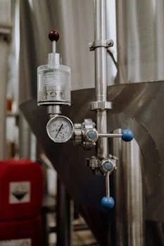
The water footprint of a modern fab campus is divided into three primary streams: Ultrapure Water (UPW) production reject, local scrubber wastewater from gas abatement, and cooling tower blowdown. While UPW reject is relatively clean, scrubber wastewater is heavily laden with hydrofluoric acid and fine particulates. Implementing CMP wastewater treatment solutions for semiconductor fabs allows facilities to capture these disparate streams, transforming a "massive wastewater headache" into a reliable source of process water that reduces reliance on municipal infrastructure.
Wafer Fab Wastewater Contaminant Profile: Fluoride, Silica & TDS Challenges
Local scrubber wastewater typically contains 50–100 ppm of fluoride and up to 65 ppm of silica, concentrations that exceed the limits of standard municipal treatment systems and traditional membrane processes (Veolia 2024). These contaminants are particularly problematic because they are highly variable; a sudden change in wafer cleaning recipes can cause fluoride spikes that destabilize conventional precipitation-flocculation-sedimentation stages. This variability necessitates the use of a precise chemical dosing for fluoride and silica removal to ensure consistent effluent quality before it reaches sensitive recycling membranes.
Total Dissolved Solids (TDS) levels in fab wastewater have increased by an average of 20% since 2020 as advanced nodes require higher chemical volumes (IEEE 2024). Beyond inorganic salts, the presence of chelating agents like EDTA and organic solvents such as Tetramethylammonium hydroxide (TMAH) introduces significant biological fouling risks. These organics serve as a food source for bacteria, leading to rapid biofilm growth on RO membranes. Managing this risk requires robust pre-oxidation or the use of an on-site ClO₂ generation for biological fouling control to maintain system flux and reduce cleaning frequency.
| Contaminant | Typical Range (ppm) | Source | Treatment Challenge |
|---|---|---|---|
| Fluoride (F-) | 50 – 150 | HF cleaning / Local scrubbers | Scaling risk; requires precipitation or EDR removal. |
| Silica (SiO2) | 40 – 80 | CMP and scrubber streams | Severe RO membrane scaling; limits recovery rates. |
| TDS | 500 – 2,500 | UPW reject / Cooling blowdown | Increases osmotic pressure; requires high-pressure RO. |
| TMAH | 10 – 100 | Photoresist developing | Toxicity to bio-systems; high nitrogen loading. |
| Chelating Agents | 5 – 20 | Post-CMP cleaning | Interferes with metal precipitation; causes bio-fouling. |
Wafer Fab Wastewater Recycling Technologies: EDR, RO & FO Compared
Electrodialysis Reversal (EDR) removes 90–95% of fluoride and silica by using an electrical potential to move ions through selective membranes, a process that is significantly more resistant to silica scaling than pressure-driven systems (Veolia 2024). Unlike RO, which pushes water through a membrane and leaves contaminants behind, EDR moves the contaminants out of the water. This makes it the preferred technology for "local scrubber reclaim" (LSR) where silica concentrations are high. However, EDR does not remove uncharged organic molecules, meaning it must often be paired with other technologies for full-stream recycling.
Reverse Osmosis (RO) remains the industry standard for TDS removal, achieving 95–98% efficiency. Modern high-efficiency RO systems for semiconductor wastewater recycling utilize advanced membranes designed specifically for high-fouling environments. The primary limitation for RO in fabs is the "silica limit"; once silica reaches saturation in the brine, it precipitates and destroys the membrane. To overcome this, fabs use high-pH RO operation or intensive antiscalant dosing. Forward Osmosis (FO) is an emerging alternative that uses a high-concentration draw solution to pull water across a membrane, offering 90%+ recovery with lower fouling potential, though it requires a complex recovery system to separate the product water from the draw solute (SAMCO 2023).
| Technology | Fluoride Removal (%) | Silica Removal (%) | TDS Removal (%) | Energy Use (kWh/m³) | CAPEX ($/m³/h) |
|---|---|---|---|---|---|
| EDR | 90 – 95% | 85 – 92% | 80 – 90% | 0.8 – 1.5 | $25,000 – $40,000 |
| RO | 95 – 98% | 95 – 99%* | 98 – 99.5% | 1.2 – 2.5 | $15,000 – $30,000 |
| FO | 90 – 95% | 90 – 95% | 99%+ | 2.0 – 4.0 | $40,000 – $60,000 |
*RO silica removal is high but limited by scaling thresholds in the concentrate stream.
Zero-Liquid-Discharge (ZLD) Systems for Wafer Fabs: Process Design & Cost Breakdown
Zero-Liquid-Discharge (ZLD) systems combine membrane-based recovery with thermal evaporation to achieve 98%+ water recovery, leaving only solid salt cake for disposal. A typical hybrid ZLD system for semiconductor fabs follows a specific hierarchy: segregation of high-load streams, primary desalination via EDR or RO, followed by a brine concentrator and a final crystallizer. This approach minimizes the volume of water sent to the energy-intensive thermal stages, which can account for 60-70% of the total system OPEX.
For a 5 MGD fab, the CAPEX for a ZLD installation typically ranges from $8M to $12M. While the initial investment is high, the system eliminates the need for expensive discharge permits and protects the fab against tightening local wastewater limits. The OPEX for these systems is roughly $0.80–$1.20 per 1,000 gallons, primarily driven by the steam or electricity required for the crystallizer. A real-world case study of a 150 m³/h EDR + RO system for wafer fab wastewater shows that by maximizing membrane recovery to 90% before the evaporator, the "thermal load" is reduced by over 80%, drastically improving the ROI of the ZLD investment.
The Hybrid ZLD Process Flow:
- Stream Segregation: Separating HFW (Hydrofluoric Waste) and CMP wastewater to prevent cross-contamination.
- Primary Recovery (EDR): Reducing fluoride and silica concentrations to manageable levels for RO.
- Secondary Recovery (High-Recovery RO): Pushing TDS removal to 95%+ recovery.
- Brine Concentration: Using Mechanical Vapor Recompression (MVR) to reduce brine volume by 10x.
- Crystallization: Converting the final 1-2% of liquid into solid waste for landfill disposal ($200–$400/ton).
ROI Calculator: Wafer Fab Wastewater Recycling vs. Freshwater Costs
Justifying a wafer fab wastewater recycling project requires a clear comparison between the rising costs of municipal freshwater and the operational costs of the recycling plant. Recycling systems typically reduce freshwater demand by 40–60%, which, when combined with avoided discharge fees, creates a compelling financial case. The ROI is calculated by determining the "Net Annual Savings" and dividing the total CAPEX by that figure.
ROI Formula:
Annual Savings = [(Freshwater Cost/kgal + Discharge Cost/kgal) - Recycling OPEX/kgal] × Annual Water Volume - Maintenance Reserve.
| Fab Size (MGD) | Freshwater + Discharge Cost ($/1,000 gal) | Recycling OPEX ($/1,000 gal) | Annual Savings (Est.) | Payback Period (Years) |
|---|---|---|---|---|
| 1 MGD | $5.50 | $2.10 | $1,241,000 | 2.5 – 4.0 |
| 5 MGD | $6.00 | $1.85 | $7,573,000 | 3.0 – 5.0 |
| 10 MGD | $7.50* | $1.70 | $21,170,000 | 2.0 – 3.5 |
*Includes drought surcharges and high-volume discharge penalties.
Decision Framework: Selecting the Right Recycling System for Your Fab
Selecting the optimal recycling architecture depends on three variables: the concentration of scaling ions (silica/fluoride), the required recovery percentage, and local discharge regulations. For facilities with relatively low-load wastewater (Fluoride < 50 ppm, Silica < 30 ppm), a standard two-stage RO system is the most cost-effective path. This setup carries a lower CAPEX ($1.5M–$3M for 5 MGD) and provides high-quality permeate suitable for cooling tower makeup or pre-treatment for UPW.
If the fab deals with high-strength scrubber wastewater (Fluoride > 50 ppm), an EDR-led system is mandatory to prevent terminal membrane scaling. This "EDR + RO" configuration increases CAPEX to the $4M–$6M range but ensures the system can handle the chemical variability of 2025-era manufacturing nodes. Finally, if the fab is located in a region with "Zero Discharge" mandates or extreme water scarcity, the addition of an MVR evaporator and crystallizer is necessary, adding approximately $3M–$5M to the project cost but providing total water independence.
Decision Logic:
- Step 1: Is Fluoride > 50 ppm or Silica > 40 ppm?
- Yes: Implement EDR as primary recovery.
- No: Utilize high-efficiency RO.
- Step 2: Is the required recovery rate > 95%?
- Yes: Add Brine Concentrator/FO.
- No: Standard membrane recovery is sufficient.
- Step 3: Is ZLD compliance required by local EPA/Municipal code?
- Yes: Integrate final Crystallizer stage.
- No: Discharge concentrated brine (if permits allow).
Frequently Asked Questions
What is the typical recovery rate for wafer fab wastewater recycling systems?
Most advanced systems achieve 90–95% recovery by combining EDR and RO. Full ZLD systems can reach 98%+, with the remaining 2% lost as moisture in the solid salt cake (DuPont 2024).
How much does a wafer fab wastewater recycling system cost?
CAPEX ranges from $1.5M for a 1 MGD RO-only system to $12M for a 10 MGD ZLD system. OPEX typically fluctuates between $1.50 and $2.50 per 1,000 gallons of treated water depending on energy costs and chemical consumption.
What are the main challenges in recycling wafer fab wastewater?
The primary technical hurdles are high silica concentrations (which cause irreversible membrane scaling) and biological fouling caused by organic solvents like TMAH. Specialized pre-treatment and EDR technology are the standard solutions for these issues (Veolia 2024).
Can recycled water be used for UPW production?
Yes. Permeate from recycling systems is often higher quality than municipal feed water. However, it requires additional polishing via ion exchange (IX), UV sterilization, and ultrafiltration (UF) to meet ASTM D5127-13 standards for semiconductor grade water.
What are the regulatory requirements for wafer fab wastewater discharge?
Discharge limits are tightening globally. Current standards typically range from 4 ppm fluoride in the US (EPA) to 5 ppm in Taiwan and 10 ppm in the EU. Many local municipalities are now imposing TDS limits, which is driving the move toward ZLD.