Wafer Fab Wastewater Engineering Solutions: 2026 Process Design, Cost Data & Zero-Liquid-Discharge Blueprint
Engineering Solutions & Case Studies
Zhongsheng Engineering Team
Wafer fab wastewater engineering solutions in 2025 must address high-concentration contaminants like fluoride (50–100 ppm), silica (65 ppm), and heavy metals while enabling water reuse or zero-liquid-discharge (ZLD). Advanced oxidation processes (AOP) like UV oxidation degrade toxic organics, while electrodialysis reversal (EDR) removes fluoride and silica with 95%+ efficiency. CAPEX for a 150 m³/hour system starts at $2.5M, with OPEX ranging from $0.30–$0.80/m³ depending on recovery rates. This guide provides contaminant-specific process designs, cost breakdowns, and a ZLD decision framework for semiconductor fabs.
Why Wafer Fab Wastewater Demands Custom Engineering Solutions
Semiconductor fabrication plants are among the most water-intensive industrial facilities globally, typically withdrawing between 2 and 4 million gallons of water per day. According to Semiengineering data, approximately 80% of this water is recirculated internally, but the remaining 20% presents a complex chemical profile that standard municipal treatment cannot handle. The wastewater is characterized by high variability in flow and concentration, containing a mix of hydrofluoric acid (HF), abrasive silica from Chemical Mechanical Planarization (CMP), and toxic heavy metals.
The primary contaminants requiring specialized engineering include fluoride (50–100 ppm), silica (65 ppm), arsenic, chromium, copper, nickel, and organic chelates. In a recent project involving a 150 m³/hour capacity facility, engineers utilized segregated stream treatment to reduce fluoride discharge violations by 98%. This granular approach is becoming mandatory as regulatory pressure intensifies. For instance, the EPA has established PFAS limits as low as 4 ppt, and the EU Industrial Emissions Directive has tightened standards for organic compounds, forcing fabs to move beyond simple precipitation toward integrated RO systems for water reuse in semiconductor fabs.
The economic impact of non-compliance is no longer limited to fines. In water-scarce regions like Taiwan or Arizona, failure to meet water recovery mandates—such as Taiwan’s 2025 ZLD requirements—can lead to production halts or the denial of permits for fab expansions. Custom engineering solutions mitigate these risks by stabilizing the treatment process against the inherent volatility of wafer fabrication cycles, ensuring that effluent consistently meets both internal reuse standards and external environmental benchmarks.
Contaminant-Specific Treatment Processes: Engineering Specs and Removal Efficiencies
Wafer fab wastewater systems must match specific technologies to the chemical profile of the influent. Fluoride and silica removal represent the most significant hurdles due to their tendency to cause scale in downstream membrane systems. Electrodialysis reversal (EDR) has emerged as a preferred solution, achieving 95%+ removal efficiency for fluoride at concentrations of 50–100 ppm. Unlike traditional calcium precipitation, EDR allows for high water recovery without the massive sludge generation associated with lime dosing.
Organic chelates and toxic organics, often found in cleaning and stripping solutions, require Advanced Oxidation Processes (AOP). UV oxidation at a 254 nm wavelength can degrade 90–98% of Chemical Oxygen Demand (COD) by generating hydroxyl radicals that break down complex organic chains. For heavy metals such as arsenic, chromium, copper, and nickel, a combination of automated chemical dosing for pH adjustment and coagulation in wafer fab wastewater followed by membrane filtration is required to reach parts-per-billion (ppb) compliance levels.
Contaminant
Influent (Avg)
Effluent Target
Primary Technology
Removal Rate
Fluoride
50–100 ppm
< 2 ppm
EDR / Ca Precipitation
95% – 99%
Silica
65 ppm
< 5 ppm
EDR / Specialized RO
92% – 96%
COD (Organics)
200–500 ppm
< 30 ppm
UV Oxidation (AOP)
90% – 98%
Copper (Cu)
2,000 ppb
< 10 ppb
Precipitation + UF
99.5%
Arsenic (As)
500 ppb
< 5 ppb
Ion Exchange / Adsorption
99%
The integration of these technologies is often sequential. For example, UV oxidation is frequently placed upstream of biological treatment or RO to break down inhibitory chelates that would otherwise foul membranes or kill microbial populations. For a detailed guide to HF wastewater treatment in semiconductor fabs, engineers must account for the specific UV dose (measured in mJ/cm²) and retention times necessary to ensure complete organic degradation before the water enters the reclamation loop.
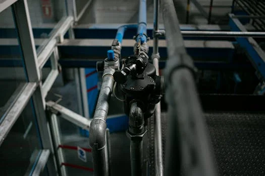
Process Flow Diagrams for Integrated Wafer Fab Wastewater Systems
wafer fab wastewater engineering solution - Process Flow Diagrams for Integrated Wafer Fab Wastewater Systems
A modern wafer fab wastewater system is rarely a single "end-of-pipe" solution. Instead, it is a series of integrated subsystems designed to handle segregated waste streams. By separating local scrubber wastewater (high HF and silica) from CMP wastewater (high abrasives) and general organic wastewater, engineers can optimize treatment efficiency and reduce chemical consumption. This segregation allows for the use of DAF systems for silica and suspended solids removal in wafer fab wastewater specifically where they are most effective.
The standard integrated process flow follows a three-stage architecture:
1. Pretreatment involves pH adjustment, screening, and equalization.
2. Primary Treatment focuses on the bulk removal of dissolved solids and organics.
3. Polishing and Recovery uses high-pressure RO for water reuse or thermal evaporation/crystallization for Zero Liquid Discharge (ZLD).
Text-Based Process Flow: Influent Streams (Scrubber/CMP/Organic) → Equalization & pH Adjustment → Primary Filtration (UF/DAF) → Contaminant Specific Removal (EDR/UV AOP) → Polishing (RO/Ion Exchange) → Final Effluent or ZLD Evaporation.
Critical control points in this flow include the UV dose verification for organic degradation and the monitoring of the Langelier Saturation Index (LSI) to prevent scaling in the RO membranes. Fail-safe valves are typically installed at the end of the primary treatment stage to divert any off-spec water back to the equalization tank, preventing contamination of the expensive polishing resins or membranes.
Zero-Liquid-Discharge vs. Water Reuse: Decision Framework and Cost Comparison
Choosing between a standard water reuse system and a full Zero-Liquid-Discharge (ZLD) blueprint depends on local water costs, land availability, and regulatory mandates. A water reuse system typically aims for 85–95% recovery, discharging a small volume of concentrated brine. In contrast, ZLD achieves 99%+ recovery by adding thermal evaporation and crystallization stages to turn the brine into solid salt cake. While ZLD eliminates discharge risks, it significantly increases both CAPEX and energy consumption.
System Type
Recovery Rate
CAPEX (150 m³/h)
OPEX ($/m³)
Best For
Standard Reuse (RO)
70% – 85%
$2M – $4M
$0.30 – $0.50
Low-cost water regions
Hybrid (EDR + RO)
85% – 95%
$4M – $8M
$0.50 – $0.80
Moderate scarcity; high silica
Full ZLD
99%+
$10M – $15M
$1.20 – $3.00
Arid regions; zero-permit zones
Decision factors for fab managers include the "true cost of water," which includes procurement, treatment, and discharge fees. In regions like Singapore or Arizona, the high cost of municipal water makes the ROI for a ZLD system design and cost breakdown for semiconductor fabs much more attractive.
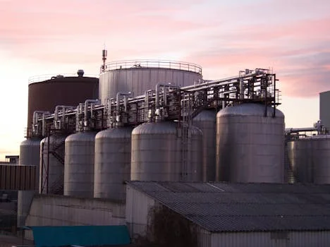
CAPEX and OPEX Breakdown: 2025 Cost Data for Wafer Fab Wastewater Systems
wafer fab wastewater engineering solution - CAPEX and OPEX Breakdown: 2025 Cost Data for Wafer Fab Wastewater Systems
Budgeting for a wafer fab wastewater system requires a granular understanding of both the initial capital investment and the long-term operational costs. For a mid-sized system with a capacity of 150 m³/hour, the CAPEX is heavily weighted toward specialized membrane stacks and automation. EDR units typically account for the largest single equipment cost due to the specialized ion-exchange membranes required for fluoride and silica removal. UV oxidation systems, while smaller in footprint, carry significant costs related to high-intensity lamps and power supply units.
Component
Estimated CAPEX
OPEX Contribution
Lifespan
EDR Stacks
$1,200,000
$0.15 / m³ (Power/Maint)
5–7 Years
UV Oxidation (AOP)
$800,000
$0.10 / m³ (Lamp/Power)
12,000 Hours (Lamps)
RO Polishing
$500,000
$0.08 / m³ (Membranes)
3 Years
Automation & PLC
$300,000
< $0.01 / m³
10 Years
Installation & Civil
$700,000
N/A
25 Years
OPEX is driven by three main factors: energy, chemicals, and component replacement. EDR systems are relatively energy-efficient, consuming about 0.5 kWh/m³, whereas RO systems can consume up to 1.2 kWh/m³ depending on the osmotic pressure of the feed. Chemical costs for pH adjustment (sulfuric acid and sodium hydroxide) can fluctuate based on the fab's production volume. To optimize ROI, many fabs are now investing in automated dosing systems that use real-time feed-forward logic to minimize chemical waste. A detailed cost breakdown for wafer fab wastewater treatment systems shows that most reuse systems pay for themselves within 4 to 6 years through reduced water and discharge fees.
Implementation Checklist: Steps to Deploy a Wafer Fab Wastewater System
Deploying a wastewater system in a live fab environment requires a phased approach to prevent production interruptions.
The following checklist provides a roadmap for process engineers and procurement teams:
Step 1: Wastewater Characterization: Conduct 24-hour composite sampling over a 30-day period to identify peak concentrations of fluoride, silica, and specific organic solvents.
Step 2: Regulatory Compliance Review: Determine the most stringent limits and ensure the design accounts for emerging PFAS regulations.
Step 3: Technology Selection: Use the decision framework to choose between ZLD, MLD, or standard reuse.
Step 4: Pilot Testing: Run a 6–12 month pilot study to assess membrane foul
Zhongsheng Engineering Team
Our team of wastewater treatment engineers has over 15 years of experience designing and manufacturing DAF systems, MBR bioreactors, and packaged treatment plants for clients in 30+ countries worldwide.