Electronics Wastewater Treatment Equipment: 2025 Engineering Specs, Hybrid DAF-RO-MBR Systems & $200K–$10M CAPEX Breakdown
Electronics manufacturing wastewater contains high levels of fluoride (50–500 mg/L), ammonia (100–1,000 mg/L), and heavy metals (copper, nickel, lead) that require specialized treatment to meet EPA and SEMI discharge limits. Hybrid DAF-RO-MBR systems achieve 95%+ water reuse and 99.9% heavy metal removal, with CAPEX ranging from $200K for small PCB lines to $10M for semiconductor fabs. Key specs: DAF TSS removal 92–97%, RO recovery 85–95%, MBR effluent COD <50 mg/L.
Why Electronics Wastewater Requires Specialized Treatment Equipment
The chemical mechanical polishing (CMP) and etching processes in semiconductor fabrication produce wastewater with silica-based slurry concentrations exceeding 2,000 mg/L and fluoride levels reaching 500 mg/L, which standard industrial filters cannot process without rapid fouling. Unlike municipal wastewater, electronics effluent is characterized by extreme fluctuations in pH and the presence of complexing agents (EDTA) that prevent heavy metals from precipitating through standard lime softening. These contaminants require a multi-stage approach to avoid violating strict regulatory thresholds.
A real-world example of the risks involved occurred in 2023, when a major semiconductor fab in Taiwan was fined $1.2 million for fluoride exceedance. The facility’s existing precipitation system failed to account for a shift in production volume, leading to fluoride discharge levels nearly double the local limit of 15 mg/L. This violation highlights the necessity of automated, high-capacity treatment trains that can handle variable influent loads while maintaining compliance with EPA 40 CFR Part 469 and SEMI S23-0719 standards.
The contaminant profile varies significantly across sub-sectors, as detailed in the following table:
| Sub-Sector | Primary Contaminants | Concentration Range (mg/L) | Regulatory Driver |
|---|---|---|---|
| Semiconductor Fab | Fluoride, Ammonia, CMP Slurry | F: 50–500; NH3: 100–1,000 | SEMI S23-0719, EPA Part 469 |
| PCB Manufacturing | Copper, Nickel, Lead, COD | Cu: 10–100; Ni: 5–50 | EPA 40 CFR Part 469 |
| Display Panel (TFT-LCD) | Indium, Tin, TMAH | TMAH: 50–200; TSS: 200–500 | Local Discharge Limits |
| Microelectronics Assembly | Photoresist, Solvents, FOG | COD: 500–2,000; FOG: 50–150 | GB 21900-2008 (China) |
Failure to treat these streams at the source results in the accumulation of toxic heavy metals in sludge and the potential for "ammonia-shocks" in biological systems, which can kill off the biomass in a Membrane Bioreactor (MBR) if not pre-treated via air stripping or ion exchange.
Contaminant Removal Technologies: How DAF, RO, and MBR Systems Work in Electronics Manufacturing

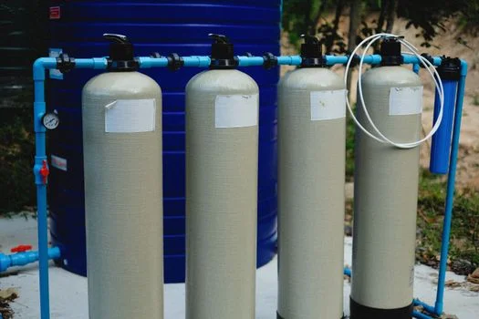
Integrated treatment trains utilize Dissolved Air Flotation (DAF) as a primary clarification stage to remove 92–97% of total suspended solids (TSS) and colloidal silica from CMP slurries. These high-efficiency DAF systems for TSS and heavy metal removal in electronics wastewater operate by injecting micro-bubbles (30–50 μm) into the influent, which attach to chemically flocculated particles and lift them to the surface for mechanical skimming. This process is critical for protecting downstream membranes from abrasive silica particles.
For dissolved ion removal, ultra-pure RO systems for fluoride and ammonia removal in semiconductor fabs are the industry standard for achieving water reuse targets. These systems utilize high-pressure (15–40 bar) thin-film composite membranes to reject 99%+ of dissolved salts. In Zero Liquid Discharge (ZLD) configurations, brine management technologies like XtremeRO or FusionRO are employed to push recovery rates beyond 95%, concentrating the remaining waste for evaporation or crystallization.
Biological contaminants and organic solvents are handled by compact MBR systems for COD and TSS removal in space-constrained electronics facilities. By combining activated sludge treatment with ultrafiltration (0.1 μm), MBRs maintain a high Mixed Liquor Suspended Solids (MLSS) concentration of 8,000–12,000 mg/L, allowing for a much smaller footprint than traditional clarifiers while producing effluent with COD levels below 50 mg/L.
| Technology | Key Engineering Parameter | Removal Efficiency | Energy Consumption |
|---|---|---|---|
| DAF | Hydraulic Loading: 5–10 m/h | TSS: 92–97% | 0.1–0.3 kWh/m³ |
| RO | Flux: 15–25 LMH | TDS/Fluoride: 98–99.5% | 2.0–4.0 kWh/m³ |
| MBR | Membrane Pore Size: 0.1 μm | COD: 90%+; TSS: 99%+ | 0.6–1.2 kWh/m³ |
| Chemical Precipitation | pH Adjustment: 9.0–11.0 | Cu: 99.9%; Ni: 95%+ | Minimal (Chemical cost high) |
Heavy metal removal specifically requires precise chemical dosing for heavy metal precipitation in PCB wastewater. By adjusting the pH to the point of minimum solubility for copper (typically pH 9.2) or nickel (pH 10.5), manufacturers can precipitate these metals as hydroxides. Advanced systems utilize sulfide precipitation to achieve even lower discharge limits, as metal sulfides are significantly less soluble than metal hydroxides across a wider pH range.
Treatment Train Comparison: Which System is Best for Your Electronics Facility?
Semiconductor fabs require water reuse targets of 95%+ to meet SEMI S23-0719 standards, necessitating a hybrid DAF-RO-MBR approach that can handle high-purity requirements and high-volume discharge. In these facilities, the DAF serves as the "workhorse" for solids removal, the MBR handles organic stripping, and the RO provides the final polishing for ultrapure water (UPW) loop makeup. This configuration (Zhongsheng field data, 2025) typically costs between $5M and $10M for a 1,000 m³/day plant but offers the highest protection against regulatory fines and water scarcity risks.
In contrast, PCB manufacturing facilities focus primarily on heavy metal compliance under EPA 40 CFR Part 469. For these plants, a combination of chemical precipitation and DAF is often sufficient for discharge compliance, though an RO stage is increasingly added for water recycling to offset municipal water costs. You can find detailed zero-discharge engineering specs for PCB wastewater treatment plants that outline how these systems achieve 90%+ water recovery with a footprint 40% smaller than conventional clarifiers.
Display panel manufacturing (TFT-LCD) introduces unique challenges, such as the removal of indium and tin. These processes benefit from hybrid DAF-RO systems integrated with selective ion exchange resins. For more technical data, see the engineering specs for display panel wastewater treatment systems which cover TMAH (Tetramethylammonium hydroxide) degradation and high-recovery RO configurations.
| Facility Type | Recommended Train | Water Recovery | Avg. CAPEX | Avg. OPEX |
|---|---|---|---|---|
| Semiconductor | DAF + MBR + RO + ZLD | 95–98% | $5M–$10M | $1.50–$2.00/m³ |
| PCB Assembly | Chem-Precip + DAF + RO | 85–90% | $200K–$1M | $0.50–$1.00/m³ |
| Display Panel | DAF + Ion Exchange + RO | 90–95% | $1M–$5M | $1.00–$1.50/m³ |
CAPEX and OPEX Breakdown: How Much Does Electronics Wastewater Treatment Equipment Cost?
Hybrid treatment systems for semiconductor fabs can reach a CAPEX of $10M depending on flow rates and zero-liquid discharge (ZLD) requirements. The equipment cost itself usually accounts for 60-70% of the total project budget, with the remainder allocated to installation, piping, and PLC-based automation systems. For a standard 500 m³/day system, the DAF unit typically ranges from $50K to $500K, while the RO and MBR units represent the bulk of the investment due to membrane costs and high-pressure pump requirements.
Operational expenditures (OPEX) are driven largely by energy consumption and chemical dosing. Automated systems can reduce chemical consumption by 30% through real-time ORP and pH monitoring. A typical OPEX breakdown for a hybrid system includes:
- Energy: $0.20–$0.80/m³ (Primarily RO high-pressure pumps and MBR aeration).
- Chemicals: $0.10–$0.50/m³ (Coagulants, polymers, and pH adjusters).
- Membrane Replacement: $0.05–$0.20/m³ (Based on a 3-year lifespan for RO and 5-year for MBR).
- Labor/Maintenance: $0.10–$0.30/m³ (Automated systems require ~10-15 hours of weekly oversight).
The Return on Investment (ROI) for these systems is often realized within 4 to 6 years. For example, a semiconductor fab treating 500 m³/day with a $5M CAPEX and $1.50/m³ OPEX can save approximately $0.80/m³ in raw water procurement and $1.20/m³ in discharge fees. When factoring in the avoidance of potential regulatory fines (which can exceed $10,000 per day per violation), the payback period becomes even more attractive to executive procurement teams.
Compliance and Water Reuse: Meeting EPA, SEMI, and Local Standards
EPA 40 CFR Part 469 mandates copper limits of 3.38 mg/L and nickel limits of 3.98 mg/L for semiconductor subcategories, though many local municipalities impose much stricter limits (often <0.5 mg/L) to protect local POTW (Publicly Owned Treatment Works) biological processes. To ensure continuous compliance, facilities must implement multi-barrier systems where the secondary stage (RO) serves as a redundant safety net for the primary chemical treatment stage.
For water reuse, the SEMI S23-0719 standard provides a framework for energy and water efficiency in semiconductor tools. Meeting these standards requires effluent to be polished to ultrapure water (UPW) quality, often requiring resistivity levels >18 MΩ·cm and Total Organic Carbon (TOC) <50 ppb. Industrial RO water treatment systems are the primary technology used to reach these targets, often paired with UV sterilization and electrodeionization (EDI) for the final polishing loop.
Global regulations are also tightening; China’s GB 21900-2008 and the EU Industrial Emissions Directive (2010/75/EU) now require Best Available Techniques (BAT) for heavy metal recovery. Zero-discharge strategies, utilizing brine concentrators and crystallizers, are becoming the preferred solution for new "mega-fabs" to secure operating permits in water-stressed regions. These systems can achieve brine recovery rates of 90%+, leaving only a small amount of solid salt cake for landfill disposal.
Frequently Asked Questions
What is the most effective method for removing fluoride from semiconductor wastewater? The most effective method is a two-stage chemical precipitation process using calcium chloride (CaCl2) to form calcium fluoride (CaF2) precipitate, followed by a DAF unit for solids separation. This typically reduces fluoride from 500 mg/L down to 10–20 mg/L. To reach <1 mg/L for high-purity reuse, a polishing RO stage or activated alumina adsorption is required.
How much space is required for a 1,000 m³/day electronics wastewater plant? A traditional clarifier-based system would require approximately 800–1,000 square meters. However, by using a hybrid MBR-RO system, the footprint can be reduced by 40–50% (approx. 400–600 square meters) because the MBR eliminates the need for large secondary clarifiers and the DAF has a much higher surface loading rate than gravity thickeners.
Can RO membranes handle CMP slurry? Directly, no. CMP slurry contains colloidal silica which will cause irreversible fouling and physical abrasion of RO membranes within hours. CMP wastewater must be pre-treated using DAF with specific coagulants or ceramic ultrafiltration (UF) to remove all suspended solids and turbidity before the water enters the RO stage.
What is the typical lifespan of membranes in an electronics environment? With proper pre-treatment (DAF and microfiltration), RO membranes in electronics applications typically last 3 to 5 years. MBR membranes, which are more robust, generally last 5 to 7 years. Lifespan is highly dependent on the effectiveness of the Clean-in-Place (CIP) protocols and the consistency of the chemical pre-treatment.