Why Third-Generation Semiconductor CMP Wastewater Demands Specialized Treatment
Third-generation semiconductor CMP wastewater contains copper (2–200 ppm), silica nanoparticles (50–250 nm), and hydrogen peroxide, requiring treatment to meet discharge limits (<2.07 ppm Cu) and enable zero liquid discharge (ZLD). On-site electrochemical systems achieve 99.9% copper recovery at ~3500 gal/week throughput, reducing off-site disposal costs by 70–80% while automating compliance. For ZLD, hybrid systems combining DAF (95% TSS removal), MBR (COD <50 mg/L), and RO (95% water recovery) deliver effluent suitable for reuse in cooling towers or ultrapure water makeup. This specific composition makes conventional "one-size-fits-all" industrial treatment systems obsolete for fabs producing Silicon Carbide (SiC) and Gallium Nitride (GaN) wafers.
Chemical Mechanical Planarization (CMP) in third-generation semiconductor manufacturing is more intensive than traditional silicon processes, often requiring higher slurry volumes and more aggressive chemical oxidizers. According to 2025 HORIBA technical data, the abrasive particles in these slurries typically range from 50 to 250 nanometers. When these particles mix with dissolved copper and benzotriazole (BTA)—a common corrosion inhibitor—they form stable, colloidal complexes that resist standard settling techniques. the presence of hydrogen peroxide (H2O2) at concentrations of 50–500 ppm poses a significant threat to biological treatment stages, as it can oxidize microbial membranes in Membrane Bioreactors (MBR) if not pre-treated.
Regulatory drivers are tightening globally, leaving fabs with little margin for error. The EPA copper discharge limit of <2.07 ppm is a baseline; however, local permits in semiconductor hubs like Taiwan (Taiwan EPA) and China (GB 21900-2008) often demand levels below 1.0 ppm. Failure to comply results in more than just fines ranging from $10,000 to $50,000 per violation; it can lead to operational shutdowns. With off-site disposal fees climbing to $2.00 per gallon in some regions, the financial burden of "hauling away the problem" is becoming a primary driver for on-site copper recovery systems for semiconductor wastewater.
CMP Wastewater Treatment Technologies: Side-by-Side Comparison
Chemical mechanical polishing (CMP) wastewater accounts for approximately 30–40% of the total wastewater volume in a modern semiconductor fab, necessitating a technology selection process that balances footprint with removal efficiency. Conventional chemical precipitation, while low in initial capital expenditure ($50K–$200K), frequently fails to meet modern ultra-low copper limits because it cannot effectively break the copper-BTA bond. This results in the generation of large volumes of hazardous "copper hydroxide" sludge that is expensive to transport and treat off-site.
Electrochemical recovery has emerged as a high-efficiency alternative for metal-rich streams. By utilizing anodic oxidation and cathodic deposition, these systems can achieve 99.9% copper removal, turning a waste stream into a 99% pure copper product that can be sold for scrap. However, while electrochemical systems excel at metal recovery, they do not address the high levels of suspended solids (silica) or organic loads (BTA) present in the slurry. To manage the total waste profile, engineers must pair recovery with robust solids removal and biological polishing.
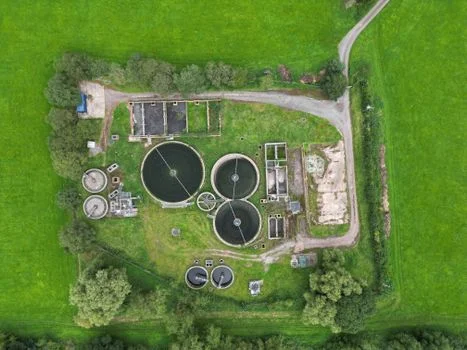
For high-volume solids removal, the ZSQ series DAF system for CMP wastewater silica and TSS removal is the industry standard. It achieves up to 95% Total Suspended Solids (TSS) removal by using micro-bubbles to float silica nanoparticles to the surface. When integrated with an integrated MBR system for COD/BOD reduction in semiconductor wastewater, the system can handle the complex organic components that remain. The MBR provides a 60% smaller footprint compared to traditional activated sludge systems, making it ideal for the space-constrained environments of cleanroom facilities.
| Technology | Primary Target | Removal Efficiency | OPEX Level | Footprint |
|---|---|---|---|---|
| Electrochemical Recovery | Dissolved Copper | 99.9% | Low (Metal Credit) | Compact |
| Dissolved Air Flotation (DAF) | Silica/TSS | 90–95% | Moderate | Medium |
| Membrane Bioreactor (MBR) | COD/BTA/Organics | 85–90% | Moderate | Small |
| Chemical Precipitation | General Metals | 70–85% | High (Sludge Cost) | Large |
| Photoelectrochemical | BTA Degradation | 95% | High (Emerging) | Experimental |
Zero Liquid Discharge (ZLD) Blueprint for CMP Wastewater: Step-by-Step Integration
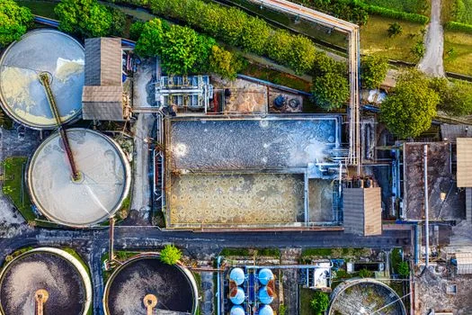
A Zero Liquid Discharge (ZLD) system for semiconductor CMP wastewater must function as a multi-stage refinery, progressively stripping contaminants until the water meets ultrapure standards for reuse. The blueprint begins with influent equalization to stabilize the fluctuating pH and chemical concentrations typical of batch CMP tool operations. Because silica nanoparticles are the most voluminous contaminant, the first critical step is solid-liquid separation. Using a ZSQ series DAF system for CMP wastewater silica and TSS removal ensures that the downstream membranes are protected from the abrasive nature of the slurry particles.
The second stage focuses on high-value heavy metal recovery in semiconductor and display panel wastewater. By placing the electrochemical recovery unit after the DAF, the electrodes are protected from fouling by silica, allowing for maximum current efficiency. Following metal recovery, the water enters a neutralization and catalytic oxidation tank where hydrogen peroxide is neutralized (often via catalase dosing) to prevent damage to the subsequent biological stage. The integrated MBR system for COD/BOD reduction in semiconductor wastewater then degrades the benzotriazole and other organic additives, reducing the Chemical Oxygen Demand (COD) to below 50 mg/L.
The final polishing stage utilizes an industrial RO system for CMP wastewater reuse and ZLD compliance. This stage removes dissolved salts and residual trace organics, achieving a permeate TDS of <10 ppm. To close the loop, the RO concentrate is processed through a plate-and-frame filter press for CMP wastewater sludge dewatering, reducing the final waste to a dry cake that represents less than 1% of the original wastewater volume. This integrated approach ensures that the fab remains in 100% compliance with EPA and EU IED standards while significantly reducing water procurement costs.
| ZLD Stage | Equipment/Technology | Target Parameter | Output Specification |
|---|---|---|---|
| 1. Pretreatment | DAF (Dissolved Air Flotation) | Silica, TSS, FOG | TSS < 20 mg/L |
| 2. Metal Recovery | Electrochemical Cell | Dissolved Cu | Cu < 0.5 ppm |
| 3. Bio-Polishing | MBR (Membrane Bioreactor) | COD, BTA, Organics | COD < 50 mg/L |
| 4. Desalination | Industrial RO System | TDS, Conductivity | TDS < 10 ppm (Reuse) |
| 5. Dewatering | Plate & Frame Filter Press | Sludge Volume | 35% Solids Cake |
Cost Breakdown: On-Site ZLD vs. Off-Site Disposal for CMP Wastewater
Off-site disposal costs for hazardous CMP wastewater can range from $0.50 to $2.00 per gallon depending on local hauling regulations and the distance to the nearest treatment facility. For a mid-sized SiC fab generating 50,000 gallons of CMP wastewater per month, the annual cost of off-site disposal can exceed $600,000. This figure does not include the "hidden" costs of environmental liability, potential permit surcharges, or the operational risk associated with third-party logistics. In contrast, an on-site ZLD system provides a fixed-cost environment that insulates the fab from rising disposal fees and regulatory shifts.
The CAPEX for a comprehensive on-site ZLD system—including DAF, electrochemical recovery, MBR, and RO—ranges from $1.2M to $2.5M for a capacity of 50–200 m³/day. While this is a significant upfront investment, the ROI is typically realized within 3 to 5 years. The primary drivers for ROI are the elimination of hauling fees, the recovery of high-purity copper (valued at $2–$10/lb depending on market rates), and the reduction in raw water intake costs. By reusing treated effluent in cooling towers, fabs can save between $0.10 and $0.30 per gallon on water procurement and discharge fees.
| Cost Category | Off-Site Disposal (Annual) | On-Site ZLD (Annual) | Savings/Benefit |
|---|---|---|---|
| Treatment/Hauling Fees | $450,000 - $900,000 | $0 | 100% Reduction |
| Chemicals/Energy | $0 | $45,000 - $85,000 | System OPEX |
| Water Procurement | $35,000 | $7,000 | 80% Reduction |
| Metal Recovery Credit | $0 | ($12,000 - $25,000) | Revenue Stream |
| Total Est. Cost | $485,000 - $935,000 | $40,000 - $67,000 | ROI in 2.8 - 4.5 Years |
Case Study: 99.9% Copper Recovery at a SiC Fab in Taiwan
A 200 mm Silicon Carbide (SiC) foundry in Taiwan reduced its copper discharge from 150 ppm to less than 0.5 ppm using an integrated electrochemical and membrane system. The facility was struggling with inconsistent influent parameters from its CMP lines, which frequently caused its legacy chemical precipitation system to fail, resulting in Taiwan EPA fines exceeding $50,000 annually. The facility required a solution that could handle 3500 gallons per week while ensuring that water was recovered for use in the plant’s cooling tower network.
The implemented solution utilized a multi-stage approach: a DAF unit for primary silica removal, followed by an electrochemical recovery system for copper. The electrochemical unit achieved 99.9% copper removal, producing a high-purity copper plate that the fab sold back to its supplier. To handle the high BTA concentrations, an MBR was installed, preceded by a catalase dosing station to neutralize hydrogen peroxide. The final stage was a low-pressure RO system that polished the water for reuse. This RO system selection for semiconductor wastewater reuse was critical, as the permeate needed to meet strict conductivity limits for the cooling towers.
The results were immediate. Beyond achieving 100% compliance with local discharge permits, the fab achieved an 80% water reuse rate. The system's automation reduced labor requirements by 60% compared to the chemical precipitation process. Most notably, the combination of metal recovery credits and the elimination of off-site disposal fees allowed the system to pay for itself in exactly 2.5 years. The fab manager noted that the hydrogen peroxide pretreatment was the "lesson learned" of the project; without it, the MBR performance would have been compromised within weeks of startup.
How to Select the Right CMP Wastewater Treatment System: Decision Framework
Selecting a treatment system based on peak flow rather than average flow prevents membrane fouling and system bypass during high-production cycles. For semiconductor EHS managers and procurement teams, the decision framework must begin with a comprehensive analysis of the CMP slurry chemistry. Because different slurries use different oxidizers and inhibitors, a system designed for a silicon process may fail when applied to GaN or SiC production. The following steps provide a technical path to selecting a zero-risk system:
- Step 1: Quantify Peak Throughput: Match system capacity to the fab’s maximum possible CMP wastewater volume. For a 3500 gal/week output, a system with a 13.2 m³/day capacity is the minimum requirement to avoid equalization tank overflow.
- Step 2: Prioritize Contaminants: If copper is the primary compliance risk, prioritize electrochemical systems. If silica-induced fouling is the main operational bottleneck, invest in a high-efficiency ZSQ series DAF system for CMP wastewater silica and TSS removal.
- Step 3: Assess ZLD Requirements: Determine if local regulations or water scarcity mandate ZLD. If so, a multi-stage system including an integrated MBR system for COD/BOD reduction in semiconductor wastewater and RO is non-negotiable.
- Step 4: Evaluate Footprint and Integration: Compare MBR systems against conventional activated sludge. MBRs offer a significant space advantage, which is critical for fabs looking to install treatment equipment within existing facility shells.
- Step 5: Pilot Testing: Never commit to a full-scale ZLD system without a 3-month pilot test. Use containerized DAF or MBR units to validate removal efficiencies on your specific waste stream before finalizing CAPEX.
Frequently Asked Questions
What is the copper discharge limit for CMP wastewater?
The federal EPA limit is <2.07 ppm, but local municipal permits in semiconductor-heavy regions like Taiwan or California often set stricter limits between 0.5 ppm and 1.0 ppm. Advanced electrochemical systems are required to consistently hit these lower targets.
Can CMP wastewater be reused in semiconductor manufacturing?
Yes. By using a ZLD blueprint that includes RO and advanced oxidation, CMP wastewater can be reclaimed for use in cooling towers, scrubbers, or as makeup water for ultrapure water (UPW) systems, provided the TDS is kept below 10 ppm.
How much does an on-site CMP wastewater treatment system cost?
CAPEX typically ranges from $1.2M to $2.5M for a full ZLD setup. However, when compared to off-site disposal costs of $1.00+/gallon, these systems offer a 3–5 year ROI through water savings and metal recovery credits.
How do you remove benzotriazole (BTA) from CMP wastewater?
BTA is best removed through a combination of electrochemical oxidation and biological treatment in an MBR. Emerging photoelectrochemical methods using BiVO4-coated WO3 anodes are also showing promise for degrading complex azole compounds.
Why does hydrogen peroxide affect wastewater treatment?
Hydrogen peroxide is a strong oxidizer that can kill the beneficial bacteria in biological systems like MBRs. It must be neutralized using chemical reducing agents or catalytic dosing (such as catalase) prior to the biological stage.
Related Guides and Technical Resources
Explore these in-depth articles on related wastewater treatment topics: