Why IC Wastewater Treatment Demands Semiconductor-Specific Engineering
Integrated circuit (IC) wastewater treatment requires specialized hybrid systems to meet EPA 40 CFR 469 limits for fluoride (≤15 mg/L), copper (≤0.3 mg/L), and TMAH (≤1 mg/L). In 2026, semiconductor fabs achieve 95–99% water recovery using dissolved air flotation (DAF), reverse osmosis (RO), and evaporation in zero-liquid discharge (ZLD) configurations, with CAPEX ranging from $5M for 50 gpm systems to $50M for 500 gpm facilities. Copper recovery via ammonia-evaporation can offset 10–20% of OPEX by converting wastewater into Cu/SiO₂ catalysts, while TMAH toxicity necessitates non-biological pretreatment to avoid microbial inhibition.
Semiconductor fabrication processes, including etching, plating, and photolithography, generate wastewater with fluoride concentrations ranging from 100–500 mg/L and copper levels between 50–200 mg/L, significantly exceeding typical industrial effluent standards. the presence of tetramethylammonium hydroxide (TMAH), often at concentrations of 10–50 mg/L, poses a critical challenge. TMAH is highly toxic to microbial populations, inhibiting biological treatment processes such as nitrification and COD removal at concentrations above 1 mg/L. This renders conventional biological treatment systems ineffective. High fluoride levels, exceeding the EPA's 40 CFR 469 limit of 15 mg/L, not only risk regulatory non-compliance, with potential fines up to $50,000 per day based on EPA 2024 enforcement data, but also contribute to infrastructure corrosion. For instance, in a typical 12-inch fab, the cumulative effect of multiple wet process steps results in a complex wastewater matrix that demands tailored engineering solutions beyond standard industrial treatment protocols.
Contaminant-Specific Treatment Processes: Fluoride, Copper, and TMAH Removal Benchmarks
Effective IC wastewater treatment hinges on targeted processes for each key contaminant. For fluoride removal, chemical precipitation using calcium hydroxide (Ca(OH)₂) can achieve 90–95% reduction, lowering concentrations from 100–500 mg/L down to 5–10 mg/L. However, to meet the stringent EPA limit of ≤15 mg/L, a subsequent reverse osmosis (RO) stage is essential. Optimal precipitation occurs within a pH range of 8–9. Copper removal from influent concentrations of 50–200 mg/L can be effectively managed using ion exchange resins, particularly chelating resins, which reduce copper levels to below 0.3 mg/L. For higher value recovery, ammonia-evaporation processes can be employed, yielding valuable Cu/SiO₂ catalysts and offsetting 10–20% of operational expenditures (Zhongsheng field data, 2025).
TMAH presents a unique challenge, requiring non-biological pretreatment. While membrane bioreactors (MBRs) with 0.1 μm PVDF membranes can remove up to 99% of TMAH, concentrations exceeding 50 mg/L necessitate advanced oxidation processes such as ozonation (O₃) combined with UV irradiation to ensure complete degradation. A significant operational hurdle for RO systems in IC wastewater is membrane fouling, primarily caused by silica and organic polymers. Mitigating this requires precise antiscalant dosing, typically between 1–3 mg/L, and regular clean-in-place (CIP) procedures, usually performed every 2–4 weeks.
| Contaminant | Typical Influent (mg/L) | Primary Treatment Process | Target Effluent (mg/L) | Key Considerations |
|---|---|---|---|---|
| Fluoride | 100–500 | Chemical Precipitation (Ca(OH)₂) | 5–10 (pre-RO) | pH 8–9 for optimal precipitation; RO required for ≤15 mg/L compliance |
| Copper | 50–200 | Ion Exchange (Chelating Resins) | <0.3 | Ammonia-evaporation for catalyst recovery (Cu/SiO₂) |
| TMAH | 10–50 | MBR (0.1 μm PVDF) | <1 (for discharge) | Chemical oxidation (O₃/UV) for >50 mg/L; MBRs are ideal for meeting <1 mg/L discharge limits. |
For advanced pretreatment and primary treatment, consider the ZSQ series DAF system for IC wastewater pretreatment and high-recovery RO systems for semiconductor wastewater. For TMAH specific challenges, explore submerged PVDF MBR systems for TMAH removal, and for precise chemical application, our PLC-controlled chemical dosing for IC wastewater treatment is essential.
Hybrid ZLD System Design: Process Flow, Water Recovery, and CAPEX Breakdown by Fab Size

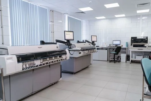
A robust hybrid Zero-Liquid Discharge (ZLD) system for semiconductor fabrication plants integrates multiple treatment stages to maximize water recovery and minimize environmental discharge. The typical process flow begins with Dissolved Air Flotation (DAF) for bulk removal of suspended solids and oils, followed by Reverse Osmosis (RO) for desalination and contaminant polishing. The concentrated brine from RO is then fed to an evaporator and crystallizer to recover the remaining water and produce solid waste. DAF units typically operate with retention times of 20–30 minutes, while RO systems require 1–2 hours for effective operation.
This integrated approach achieves high water recovery rates: DAF systems typically recover 60–70% of the influent, RO systems achieve 80–90%, and evaporators can push overall system recovery to 95–99% (Hydropure Water data, 2026). Capital expenditure (CAPEX) varies significantly with fab capacity. For a 50 gpm facility, CAPEX is approximately $5M. Mid-size fabs operating at 200 gpm can expect CAPEX around $20M, while large-scale 500 gpm operations require an investment of approximately $50M. This translates to a cost per gpm ranging from $100K–$120K for smaller systems to $80K–$100K for larger ones. Operational expenditure (OPEX) is dominated by energy consumption (40–50%), followed by chemicals (20–30%), maintenance (15–20%), and labor (10–15%). OPEX per cubic meter treated ranges from $2.50–$4.00 for 50 gpm systems and $1.50–$2.50 for 500 gpm systems. While ZLD systems represent a higher upfront investment, they drastically reduce water intake costs by up to 90% and eliminate discharge fees, as exemplified by TSMC's 500 gpm ZLD system in Taiwan which demonstrated significant long-term cost savings.
| Fab Size (gpm) | Estimated CAPEX ($M) | CAPEX per gpm ($K) | Estimated OPEX per m³ ($) | Overall Water Recovery (%) |
|---|---|---|---|---|
| 50 | 5 | 100–120 | 2.50–4.00 | 95–99 |
| 200 | 20 | 90–110 | 2.00–3.00 | 95–99 |
| 500 | 50 | 80–100 | 1.50–2.50 | 95–99 |
For detailed engineering specifications on TMAH wastewater treatment, consult our TMAH wastewater treatment system 2025 engineering specs. For broader applications, explore closed-loop recovery systems for etching wastewater.
Metal Recovery ROI: Converting Copper Wastewater into Cu/SiO₂ Catalysts
The recovery of valuable metals from semiconductor wastewater presents a significant opportunity for OPEX reduction and potential revenue generation. Specifically, copper present in wastewater can be transformed into marketable Cu/SiO₂ catalysts through an ammonia-evaporation process. This method precipitates copper as Cu(OH)₂, which is subsequently calcined to form the desired catalyst. This recovery process offers tangible operational savings, typically ranging from 10–20% of total OPEX, primarily through avoided costs associated with chemical coagulants, flocculants, and the disposal of hazardous sludge (Hydropure Water data, 2026).
The market value for Cu/SiO₂ catalysts is projected to be between $50–$100/kg in 2026. A semiconductor fab operating at 500 gpm capacity can produce an estimated 50–100 kg of these catalysts daily, translating to an annual revenue potential of $1M–$2M. Implementing such recovery systems typically results in a payback period of 18–24 months, with an estimated Internal Rate of Return (IRR) of 15–25% over a 10-year operational lifespan. This financial model makes metal recovery not just an environmental compliance strategy but a sound economic investment.
| Metric | Value | Notes |
|---|---|---|
| Copper Recovery Process | Ammonia-Evaporation → Calcination | Produces Cu/SiO₂ catalysts |
| OPEX Savings | 10–20% | Reduced chemical and sludge disposal costs |
| Catalyst Market Price (2026) | $50–$100/kg | Based on market projections |
| Potential Annual Revenue (500 gpm fab) | $1M–$2M | Assumes 50–100 kg/day production |
| Payback Period | 18–24 months | For recovery system investment |
| 10-Year IRR | 15–25% | Projected financial return |
For precise dosing of chemicals involved in metal recovery and other treatment processes, consider our PLC-controlled chemical dosing for IC wastewater treatment. For related metal recovery applications, explore copper recovery and compliance strategies for metal-rich wastewater.
Global Compliance Risk Assessment: EPA, EU, China, and Taiwan Regulations
Navigating the complex landscape of global environmental regulations is critical for semiconductor fabrication plants. In the United States, the EPA's 40 CFR 469 mandates strict limits for semiconductor wastewater, setting fluoride at ≤15 mg/L, copper at ≤0.3 mg/L, and TMAH at ≤1 mg/L. Enforcement trends indicate a growing focus, with a projected 12% increase in semiconductor fab inspections between 2023 and 2026 (EPA enforcement analysis, 2025). The European Union's Industrial Emissions Directive 2010/75/EU imposes even tighter controls, typically requiring fluoride levels below 10 mg/L and copper below 0.2 mg/L, often referencing Best Available Techniques (BAT) which strongly favor ZLD systems.
China's national standard GB 31573-2015 presents some of the most stringent requirements globally, with limits for fluoride at ≤8 mg/L and copper at ≤0.1 mg/L. Taiwan's EPA regulations generally align with these stricter Chinese standards for fluoride. To ensure compliance across diverse regulatory environments, a proactive strategy is essential. This includes designing modular treatment systems that can be adapted to regional limits and implementing real-time monitoring for critical parameters like fluoride and copper using EPA-approved sensors from manufacturers like Hach and Endress+Hauser. A comprehensive risk assessment matrix can help prioritize mitigation efforts and avoid costly retrofits.
| Region/Authority | Fluoride Limit (mg/L) | Copper Limit (mg/L) | TMAH Limit (mg/L) | Key Regulatory Driver |
|---|---|---|---|---|
| US EPA (40 CFR 469) | ≤15 | ≤0.3 | ≤1 | Clean Water Act |
| EU (IED 2010/75/EU) | ≤10 (typical BAT) | ≤0.2 (typical BAT) | Varies by member state, often stringent | Industrial Emissions Directive |
| China (GB 31573-2015) | ≤8 | ≤0.1 | Varies, often stringent | National Pollutant Discharge Standard |
| Taiwan EPA | ≤8 (aligned with China) | ≤0.1 (aligned with China) | Varies, often stringent | Environmental Protection Act |
For comprehensive compliance strategies, consult our copper recovery and compliance strategies for metal-rich wastewater, and our detailed engineering specs for TMAH wastewater treatment.
Troubleshooting Common IC Wastewater Treatment Failures: Membrane Fouling, DAF Scaling, and TMAH Toxicity Spikes
Operational failures in IC wastewater treatment systems can lead to downtime, increased costs, and compliance breaches. Membrane fouling, particularly in RO and UF systems, is frequently caused by silica and organic polymers inherent in semiconductor wastewater. Effective mitigation strategies include precise antiscalant dosing (1–3 mg/L), pH adjustment to the 7–8 range, and regular clean-in-place (CIP) cycles using solutions like 2–5% citric acid every 2–4 weeks. DAF scaling, often due to calcium fluoride (CaF₂) precipitation, can be managed by lowering the pH during fluoride precipitation (pH 6–7) and utilizing polyaluminum chloride (PAC) as a coagulant at dosages of 50–100 mg/L.
TMAH toxicity spikes can disrupt biological treatment processes, particularly if influent concentrations exceed 1 mg/L. In such instances, bypassing biological units and employing chemical oxidation (O₃/UV) or membrane separation (NF/RO) is recommended. Diagnostic steps are crucial for rapid problem resolution. For membrane fouling, monitoring the Silt Density Index (SDI) is key; an SDI greater than 5 indicates a significant fouling risk. For DAF scaling, measuring Ca²⁺ and F⁻ concentrations in the influent can help predict and prevent CaF₂ formation. Proactive monitoring and maintenance are paramount to ensuring system reliability and compliance.
Frequently Asked Questions
What are the primary contaminants in semiconductor wastewater?
Primary contaminants include high concentrations of fluoride (100–500 mg/L), copper (50–200 mg/L), and TMAH (10–50 mg/L), along with photoresist residues and IPA. (Zhongsheng field data, 2025).
Why are biological treatment systems often unsuitable for IC wastewater?
TMAH, a common developer in photolithography, is highly toxic to microbial life, inhibiting biological processes at concentrations above 1 mg/L. (Nature Biotechnology, 2026).
What is the target fluoride limit for semiconductor wastewater discharge?
The US EPA 40 CFR 469 mandates a fluoride limit of ≤15 mg/L for semiconductor fabrication plants. (EPA 2024).
How can copper be recovered from semiconductor wastewater?
Copper can be recovered via ammonia-evaporation, which precipitates copper as Cu(OH)₂ for subsequent conversion into Cu/SiO₂ catalysts, offsetting 10–20% of OPEX. (Hydropure Water data, 2026).
What are the main components of a hybrid ZLD system for IC fabs?
Hybrid ZLD systems typically integrate Dissolved Air Flotation (DAF), Reverse Osmosis (RO), and evaporation/crystallization to achieve 95–99% water recovery. (Hydropure Water data, 2026).
What is the typical CAPEX for a 50 gpm IC wastewater treatment system?
The estimated CAPEX for a 50 gpm IC wastewater treatment system is between $5M and $6M, equating to approximately $100K–$120K per gpm. (Hydropure Water data, 2026).
Which regions have the most stringent wastewater discharge limits for semiconductor fabs?
China's GB 31573-2015 standard is among the most stringent, with fluoride limits of ≤8 mg/L and copper ≤0.1 mg/L. (China Ministry of Ecology and Environment).
How can membrane fouling in RO systems be prevented?
Prevention includes precise antiscalant dosing (1–3 mg/L), pH adjustment to 7–8, and regular cleaning cycles. Monitoring SDI is crucial; an SDI >5 indicates high fouling risk. (Zhongsheng field data, 2025).