Home>Blog>Industry News>Integrated Circuit Wastewater Zero Liquid Discharge: 2026 Engineering Specs, Cost Data & Hybrid ZLD System Design
Integrated Circuit Wastewater Zero Liquid Discharge: 2026 Engineering Specs, Cost Data & Hybrid ZLD System Design
Industry News
Zhongsheng Engineering Team
Integrated Circuit Wastewater Zero Liquid Discharge: 2025 Engineering Specs, Cost Data & Hybrid ZLD System Design
Integrated circuit (IC) wastewater zero liquid discharge (ZLD) systems eliminate liquid waste from semiconductor fabs by combining forward osmosis (FO), nanofiltration (NF), reverse osmosis (RO), and crystallizers to achieve 95%+ water recovery. For a 150 m³/h system, hybrid FO-NF-RO designs remove 99.5% of fluoride and silica (per 2025 EPA benchmarks), with CAPEX ranging from $2.5M to $15M depending on pretreatment needs and compliance requirements. ZLD systems are critical for fabs in water-stressed regions like Taiwan and Singapore, where discharge limits for TMAH, CMP slurry, and heavy metals are tightening.
Why Integrated Circuit Fabs Need Zero Liquid Discharge Systems
Semiconductor fabs consume between 2 and 10 million gallons of water per day, with 30–50% of this volume often discharged as complex wastewater (per SEMI 2024 data). This wastewater typically contains challenging contaminants such as tetramethylammonium hydroxide (TMAH), chemical mechanical planarization (CMP) slurry, fluoride, and heavy metals, necessitating advanced treatment solutions. Global discharge limits for IC wastewater are becoming increasingly stringent; for instance, Taiwan mandates TMAH concentrations below 1 mg/L and fluoride below 15 mg/L, while Singapore restricts silica to less than 50 mg/L. Similarly, the EU enforces heavy metal limits of less than 0.1 mg/L under Directive 2010/75/EU for industrial emissions.
A real-world example demonstrates the impact: a 2025 wafer fab in Hsinchu, Taiwan, implemented a zero liquid discharge system and subsequently reduced its fresh water intake by 40%. This proactive measure not only enhanced water security but also allowed the fab to avoid an estimated $1.2M per year in fines for potential non-compliance with evolving Taiwan EPA standards. Without ZLD systems, semiconductor manufacturing facilities face significant environmental and operational risks, including groundwater contamination, recurrent permit violations leading to substantial penalties, and potential disruptions to their supply chain due to water scarcity or regulatory shutdowns. Implementing a robust ZLD system mitigates these risks, ensuring long-term operational sustainability and compliance.
IC Wastewater Contaminant Profiles: What ZLD Systems Must Remove
integrated circuit wastewater zero liquid discharge - IC Wastewater Contaminant Profiles: What ZLD Systems Must Remove
Semiconductor wastewater streams present a complex mix of contaminants, each requiring specialized removal strategies within a ZLD system. TMAH (tetramethylammonium hydroxide), found in developer wastewater at concentrations typically ranging from 50–500 mg/L, requires precise pH adjustment (pH 10–12) followed by nanofiltration (NF) and reverse osmosis (RO) membranes to achieve over 99% removal, meeting stringent 2025 SEMI S23 standards. Chemical mechanical planarization (CMP) slurry, a significant contributor of total suspended solids (TSS) with concentrations between 1,000–5,000 mg/L (comprising silica, alumina, and ceria particles), necessitates robust primary treatment. High-efficiency DAF systems can achieve up to 95% TSS removal, while lamella clarifiers can provide 90% removal, both crucial steps before subsequent membrane stages. For fluoride, present in etching wastewater at 100–1,000 mg/L, chemical precipitation using Ca(OH)₂ is typically employed to reduce concentrations to below 15 mg/L before feeding into RO systems, aligning with EPA 40 CFR Part 469 guidelines. Heavy metals such as copper (Cu), nickel (Ni), and chromium (Cr), often found at 1–50 mg/L, demand advanced polishing steps like ion exchange or electrocoagulation to achieve 99.9% removal, meeting the strict requirements of EU Directive 2010/75/EEC. Finally, silica, with concentrations of 50–300 mg/L, requires efficient removal via RO or electrodeionization (EDI) to achieve 95% reduction, essential for producing semiconductor-grade water suitable for reuse (per ASTM D5127).
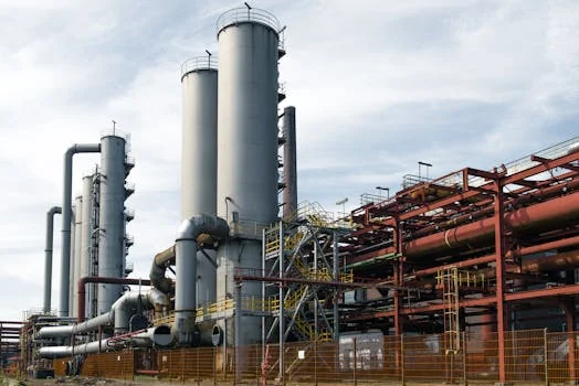
Hybrid ZLD System Designs for Semiconductor Fabs: Process Flows and Efficiency Data
Hybrid ZLD system designs are essential for achieving high water recovery and contaminant removal efficiencies in semiconductor manufacturing, combining multiple technologies to address diverse wastewater characteristics. An FO-NF-RO hybrid system, for example, typically achieves a remarkable 95% water recovery and 99.5% removal of fluoride and silica, with energy consumption ranging from 2.5–4.0 kWh/m³ (per a 2025 Veolia case study). Alternatively, an EDR-RO-crystallizer system can achieve 90% water recovery and 99.8% TMAH removal, albeit with slightly higher energy consumption of 3.0–5.0 kWh/m³ (per 2024 Dow Water & Process Solutions data).
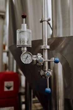
A typical process flow for a semiconductor ZLD system begins with robust pretreatment to manage high-TSS and metal-laden streams. This often involves a high-efficiency DAF system or lamella clarifier (with residence times of 2–4 hours) for initial solids reduction and pH neutralization. Following pretreatment, the water proceeds to advanced membrane stages. Forward osmosis (FO) or nanofiltration (NF) can act as a pre-concentrator, reducing the load on subsequent semiconductor-grade RO systems. The RO stage (with residence times of 1–2 hours) further concentrates dissolved solids, recovering the majority of the water. The concentrated brine from the RO is then directed to a crystallizer or evaporator, where all remaining water is recovered, leaving behind only solid waste for disposal. Membrane fouling, particularly silica scaling on RO membranes, is a significant challenge in IC wastewater ZLD. Mitigation strategies include precise antiscalant dosing, continuous pH adjustment, and regular chemical cleaning cycles. Comparing recovery rates, a single-stage RO system typically achieves 75–85% water recovery, whereas incorporating a two-stage RO process can push recovery to 90–95% in IC wastewater applications, significantly enhancing overall system efficiency. For a more in-depth look at process flows and contaminant removal, refer to this real-world IC wastewater ZLD case study with engineering specs.
System Type
Water Recovery (%)
Fluoride/Silica Removal (%)
TMAH Removal (%)
Energy Consumption (kWh/m³)
FO-NF-RO Hybrid
95+
99.5
99.0
2.5–4.0
EDR-RO-Crystallizer
90+
99.0
99.8
3.0–5.0
Thermal Evaporator (Standalone)
99+
99.9
99.9
10–20 (high thermal)
ZLD System Cost Breakdown: CAPEX, OPEX, and ROI for Semiconductor Fabs
integrated circuit wastewater zero liquid discharge - ZLD System Cost Breakdown: CAPEX, OPEX, and ROI for Semiconductor Fabs
The capital expenditure (CAPEX) for an IC fab zero liquid discharge system typically ranges from $2.5M to $15M, primarily influenced by the system's capacity (from 50 m³/h to 500 m³/h) and the complexity of pretreatment required for specific wastewater streams (per a 2025 SEMI cost survey). Operational expenditure (OPEX) is a critical ongoing cost, with energy consumption accounting for approximately 40% of the total, followed by membrane replacement at 25%, chemical consumption at 20%, labor costs at 10%, and routine maintenance at 5%.
Return on investment (ROI) for ZLD systems is driven by multiple factors. Direct water savings can range from $0.50–$2.00 per cubic meter, depending on local freshwater costs and discharge fees. Avoided regulatory fines, which can reach $100K–$1M annually, represent a significant financial incentive. Additionally, water reuse incentives, such as Singapore’s NEWater rebates, further enhance the economic viability of ZLD. A detailed cost breakdown for IC wastewater ZLD systems highlights these financial aspects. When comparing different ZLD system configurations, the cost profiles vary significantly:
System Type
Estimated CAPEX (500 m³/h system)
Estimated OPEX (per m³)
Typical Payback Period
FO-NF-RO Hybrid
$5M–$10M
$0.80–$1.50
3–5 years
EDR-RO-Crystallizer
$7M–$12M
$1.00–$1.80
4–6 years
Thermal Evaporator
$10M–$15M
$2.00–$4.00
5–7 years
For fabs with budget constraints, various financing options are available, including equipment leasing, performance-based contracts, and government subsidies for sustainable water management. These options can help mitigate the initial capital outlay and accelerate the adoption of ZLD technologies. More detailed financial analysis can be found in this detailed cost breakdown for IC wastewater ZLD systems.
Compliance Checklist: Meeting Global IC Wastewater Discharge Standards with ZLD
Meeting global IC wastewater discharge standards is a non-negotiable requirement for semiconductor fabs, and ZLD systems are designed to ensure strict compliance. In Taiwan, for example, the Taiwan EPA 2025 standards mandate that discharged wastewater must have TMAH concentrations below 1 mg/L, fluoride below 15 mg/L, and a pH maintained between 6–9. Singapore's National Environment Agency (NEA) 2024 guidelines are equally rigorous, setting limits for silica below 50 mg/L, total suspended solids (TSS) below 30 mg/L, and heavy metals below 0.1 mg/L. The European Union's Directive 2010/75/EU imposes strict limits on heavy metals (Cu, Ni, Cr) at less than 0.1 mg/L and chemical oxygen demand (COD) below 125 mg/L. In the United States, EPA 40 CFR Part 469 sets fluoride limits at less than 4 mg/L for certain categories, while EPA 40 CFR Part 403 generally limits TSS to less than 30 mg/L for industrial discharges to public sewers.
Effective ZLD system management requires comprehensive documentation. This includes maintaining daily operational logs, conducting regular third-party laboratory testing of treated effluent, and implementing continuous monitoring systems for critical parameters like pH and TSS to ensure real-time compliance verification.
Region/Standard
Key Parameters
Discharge Limit
Taiwan EPA (2025)
TMAH
< 1 mg/L
Fluoride
< 15 mg/L
pH
6–9
Singapore NEA (2024)
Silica
< 50 mg/L
TSS
< 30 mg/L
Heavy Metals
< 0.1 mg/L
EU Directive 2010/75/EU
Heavy Metals (Cu, Ni, Cr)
< 0.1 mg/L
COD
< 125 mg/L
US EPA (40 CFR Part 469/403)
Fluoride
< 4 mg/L
TSS
< 30 mg/L
Frequently Asked Questions
integrated circuit wastewater zero liquid discharge - Frequently Asked Questions
The typical payback period for a semiconductor ZLD system ranges from 3–7 years, largely dependent on local water costs, the severity of regulatory fines, and available water reuse incentives (per a 2025 SEMI ROI calculator). Yes, ZLD systems are engineered to handle high-silica wastewater from CMP processes, but they require specialized pretreatment and robust reverse osmosis (RO) or electrodeionization (EDI) units, often coupled with antiscalant dosing, to effectively prevent membrane fouling and achieve over 95% silica removal. Energy consumption benchmarks for IC fab ZLD systems generally fall between 2.5–5.0 kWh/m³, with FO-NF-RO hybrid designs typically operating at the lower end of this range due to their lower energy intensity, while thermal evaporators consume significantly more. RO membranes in ZLD systems typically require replacement every 3–5 years, though this lifespan can vary based on the quality of the feedwater pretreatment and the frequency of membrane cleaning. Yes, modular ZLD systems are available for smaller fabs, with skid-mounted units offering capacities from 50–150 m³/h and CAPEX starting at approximately $1.5M, providing flexible and scalable solutions.
Our team of wastewater treatment engineers has over 15 years of experience designing and manufacturing DAF systems, MBR bioreactors, and packaged treatment plants for clients in 30+ countries worldwide.