Home>Blog>Industry News>Wafer Fab Wastewater Discharge Standards 2026: Global Limits, Treatment Tech & Compliance Blueprint
Wafer Fab Wastewater Discharge Standards 2026: Global Limits, Treatment Tech & Compliance Blueprint
Industry News
Zhongsheng Engineering Team
Wafer Fab Wastewater Discharge Standards 2025: Global Limits, Treatment Tech & Compliance Blueprint
Wafer fab wastewater discharge standards in 2025 vary globally but share strict limits: EPA Part 469 mandates ≤10 mg/L TSS and ≤120 mg/L COD, while the EU’s Industrial Emissions Directive (IED) sets ≤5 mg/L for heavy metals like arsenic. Semiconductor plants face unique challenges—wastewater from 4,000+ processing steps lacks nutrients for biological treatment, requiring advanced tech like high-efficiency DAF systems (95%+ TSS removal) or MBR systems for near-reuse-quality effluent (99.8% contaminant reduction). Compliance demands 24/7 monitoring, as seen in TSMC’s fab protocols, and proactive re-tooling to handle evolving chemical streams.
Why Wafer Fab Wastewater Standards Are Getting Stricter in 2025
Global regulatory frameworks are tightening wastewater discharge limits for semiconductor manufacturing due to increasing environmental awareness and the industry's rapid expansion. The CHIPS Act incentivizes US fabs with funding, but these incentives are often contingent upon meeting increasingly stringent wastewater discharge requirements, as outlined in recent EPA 2024 guidance. Similarly, the EU’s Industrial Emissions Directive (IED) 2024 update lowers heavy metal limits by 30% for semiconductor plants, specifically reducing arsenic from 10 µg/L to 7 µg/L. In Asia, China’s 14th Five-Year Plan mandates zero-liquid-discharge (ZLD) for new fabs in water-scarce regions such as Beijing and Shanghai, pushing for minimal environmental impact.
Non-compliance carries substantial financial and operational risks. For instance, TSMC faced a $100 million fine in 2023 for exceeding Taiwan’s TSS limits, according to public records from the Taiwan EPA. Such penalties highlight the severe financial repercussions and potential for operational disruptions, including temporary shutdowns and reputational damage. the semiconductor industry's relentless pace of innovation means fab re-tooling for advanced nodes, such as transitioning from 3nm to 2nm, introduces new contaminants like PFAS and gallium. These emerging pollutants are often not adequately covered by legacy standards, necessitating continuous upgrades to wastewater treatment systems and vigilant monitoring to maintain compliance with evolving regulations. The constant in fab wastewater quality and quantity is change; as fabs re-tool for subsequent processing nodes, wastewater discharges will only grow in volume and complexity (Carollo, 2024).
Global Wafer Fab Wastewater Discharge Limits: 2025 Comparison Table
wafer fab wastewater discharge standard - Global Wafer Fab Wastewater Discharge Limits: 2025 Comparison Table
Meeting the most stringent global wafer fab wastewater discharge limits requires a comprehensive understanding of regional regulations. The table below provides a side-by-side comparison of key parameters for major semiconductor manufacturing hubs, enabling engineers to design robust treatment systems.
Parameter
US (EPA 40 CFR Part 469)
EU (IED 2024/2466)
China (GB 21900-2008 & 14th FYP)
Taiwan (EPA Industrial Wastewater Std)
South Korea (Water Env. Pres. Act)
Japan (Water Poll. Control Act)
TSS (mg/L)
≤10
≤5
≤3 (for ZLD fabs)
≤5
≤10
≤20
COD (mg/L)
≤120
≤50
≤30 (for ZLD fabs)
≤50
≤80
≤90
BOD (mg/L)
≤20
≤15
≤10 (for ZLD fabs)
≤15
≤20
≤30
Arsenic (µg/L)
≤10
≤7 (post-2024 update)
≤5
≤5
≤10
≤10
Copper (µg/L)
≤20
≤50
≤50
≤50
≤100
≤300
Nickel (µg/L)
≤40
≤100
≤100
≤100
≤200
≤1000
Fluoride (mg/L)
≤15
≤10
≤8
≤10
≤15
≤8
pH
6.0–9.0
6.0–9.0
6.0–9.0
6.0–9.0
6.0–9.0
5.8–8.6
PFAS
≤70 ppt (proposed)
≤0.1 µg/L (2025)
No specific limit yet
No specific limit yet
No specific limit yet
No specific limit yet
Gallium (mg/L)
No specific limit yet
No specific limit yet
No specific limit yet
≤1
No specific limit yet
No specific limit yet
This comparison highlights significant discrepancies across regions. For instance, the US EPA 40 CFR Part 469 allows 10 mg/L TSS, while the EU’s IED mandates a stricter 5 mg/L, and China requires 3 mg/L for new zero-liquid-discharge (ZLD) fabs. Emerging contaminants like PFAS are gaining regulatory attention, with the US proposing limits around 70 ppt and the EU setting a 2025 limit of 0.1 µg/L. Gallium, a crucial element in advanced semiconductor manufacturing, is specifically regulated in Taiwan at 1 mg/L, but other regions have yet to establish dedicated limits. discharge limits can vary by fab age; for example, newer facilities constructed under the US CHIPS Act often face up to 50% stricter requirements compared to grandfathered plants, emphasizing the need for forward-looking treatment strategies in 2025 chip fab wastewater engineering solutions.
How Wafer Fab Wastewater Differs from Municipal Wastewater: Treatment Challenges
Wafer fab wastewater presents unique challenges that render conventional municipal wastewater treatment systems largely ineffective. A primary distinction is the severe lack of nutrients in fab wastewater, resulting in a BOD:N:P ratio often less than 10:1:0.1, starkly contrasting with municipal wastewater’s ideal 100:5:1 ratio. This nutrient deficiency effectively starves biological treatment systems, preventing the microbial growth necessary for efficient organic contaminant removal.
Additionally, fab wastewater exhibits high variability, with chemical streams changing weekly due to re-tooling for different processing nodes. Switching from 14nm to 7nm nodes, for example, can alter fluoride and metal loads by as much as 40%, making it difficult for fixed-design biological systems to adapt. The wastewater also frequently has a low pH (typically 2–4) and contains high levels of oxidants like hydrogen peroxide and ozone, both of which are highly inhibitory or lethal to microbial populations in aeration tanks. To mitigate these issues, TSMC’s fabs often employ separate collection systems for acid and alkaline waste streams, allowing for pre-treatment and neutralization before mixing, which significantly reduces the overall cost of chemical neutralization. Understanding these fundamental differences is crucial for selecting appropriate semiconductor wastewater treatment technologies.
Characteristic
Municipal Wastewater
Wafer Fab Wastewater
pH
Neutral (6.5–7.5)
Highly Variable (2–12), often low (2–4)
TSS
Moderate (150–300 mg/L)
Low to Moderate (10–100 mg/L), often fine colloids
COD
Moderate to High (300–800 mg/L)
Low to Moderate (50–200 mg/L), high variability
BOD:N:P Ratio
Ideal for biological (100:5:1)
Nutrient deficient (<10:1:0.1)
Variability
Relatively stable
High, changes weekly with process re-tooling
Toxic Compounds
Low levels, biodegradable organics
Heavy metals, fluorides, oxidants, PFAS, complex organics
Treatment Technologies for Wafer Fab Wastewater: Process Flows and Efficiency Data
wafer fab wastewater discharge standard - Treatment Technologies for Wafer Fab Wastewater: Process Flows and Efficiency Data
Selecting the optimal treatment technology for wafer fab wastewater requires evaluating contaminant removal rates, footprint, and operational costs. A typical multi-stage treatment process often begins with stream segregation and neutralization, followed by physical-chemical and biological steps, and concluding with advanced polishing.
* Dissolved Air Flotation (DAF) Systems: High-efficiency DAF systems are critical for initial solids and oil/grease removal. Zhongsheng’s ZSQ series DAF systems typically achieve 95% TSS removal, 85% oil/grease removal, and up to 70% COD reduction. DAF units are effective for removing fine colloidal particles and minimizing downstream loading.
* Chemical Precipitation: This process is highly effective for semiconductor heavy metal wastewater treatment, achieving up to 99% removal of heavy metals such as arsenic and copper. It involves adding coagulants (e.g., ferric chloride) and flocculants to induce precipitation, followed by sedimentation. The main drawback is the generation of hazardous sludge, necessitating specialized disposal that adds to operational costs.
* Membrane Bioreactor (MBR) Systems: MBR systems combine biological treatment with membrane filtration, offering superior effluent quality. MBR systems for near-reuse-quality effluent achieve 99.8% pathogen removal and up to 95% COD reduction. While highly effective, MBR systems typically have a 30% higher CAPEX compared to DAF systems (TSMC data).
* Reverse Osmosis (RO) / Nanofiltration (NF): For facilities aiming for zero-liquid-discharge (ZLD) or water reuse, RO and NF membranes are essential. These systems can achieve over 90% water recovery, producing high-purity water suitable for industrial processes. However, RO systems incur approximately double the energy cost of DAF systems due to high-pressure requirements.
A common process flow for comprehensive wafer fab wastewater treatment includes:
1. **Acid/Alkaline Neutralization:** Adjusting pH to a neutral range (6-9) to protect downstream biological processes and facilitate metal precipitation.
2. **DAF System:** Removes suspended solids, oils, and greases (95% TSS removal).
3. **Chemical Precipitation:** Targets specific heavy metals (e.g., arsenic, copper, nickel) for removal (99% heavy metal removal).
4. **MBR System:** Provides advanced biological treatment and filtration for organic removal and pathogen reduction (95% COD, 99.8% pathogen removal).
5. **RO/NF System:** Polishes effluent for high-purity water recovery, crucial for semiconductor wastewater ZLD solutions and internal reuse (90%+ water recovery).
Technology
Primary Contaminant Target
Typical Removal Efficiency (%)
Footprint Consideration
DAF System
TSS, Oil & Grease, Colloids
TSS: 95+, O&G: 85+, COD: 70+
Moderate
Chemical Precipitation
Heavy Metals (Ar, Cu, Ni, F)
Heavy Metals: 99+, Fluoride: 90+
Moderate
MBR System
BOD, COD, TSS, Pathogens
COD: 95+, TSS: 99.8+, Pathogens: 99.8+
Compact
RO/NF System
Dissolved Solids, Salts, Trace Contaminants
TDS: 90-99+, Water Recovery: 90+
Large, energy intensive
Compliance Blueprint: Step-by-Step Engineering Specs for 2025 Standards
Achieving and maintaining compliance with stringent 2025 wafer fab wastewater discharge standards requires a proactive engineering approach. This blueprint provides a step-by-step guide for fab operators to audit their existing systems and identify necessary upgrades before regulatory inspections.
* Step 1: Stream Segregation and Pre-treatment. Effective wastewater management begins with segregating distinct waste streams at the source, as recommended by EPA 2021 guidance. Acid/alkaline streams should be kept separate from metal-bearing wastes and organic solvent wastes. This simplifies treatment by preventing unwanted reactions (e.g., precipitation of metals at high pH that might redissolve at low pH) and reduces the volume requiring specialized treatment. For instance, concentrated metal-bearing streams can undergo dedicated chemical precipitation, while high-fluoride streams may require calcium fluoride precipitation.
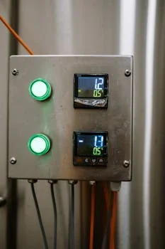
* Step 2: Real-time Monitoring with 24/7 Alerts. Continuous, real-time monitoring of critical parameters such as pH, TSS, COD, and heavy metals (e.g., arsenic, copper) is indispensable. TSMC’s fabs, for example, employ sophisticated systems with 24/7 monitoring by shift personnel and automated alerts for any excursions from permit limits (TSMC, 2021). Implementing an automatic chemical dosing system ensures immediate pH adjustment or coagulant addition in response to real-time data, preventing discharge violations.
* Step 3: Redundancy Planning and Emergency Containment. To prevent operational disruptions and abnormal discharge events, redundancy in critical equipment (e.g., pumps, blowers, chemical dosing systems) and backup power supplies are essential. EPA guidelines often require facilities to demonstrate a 2-hour response time for abnormal discharge incidents. Emergency containment basins or secondary containment for chemical storage further mitigate the risk of environmental spills, which can lead to severe penalties.
* Step 4: PFAS Treatment Integration. For fabs utilizing PFAS-based photoresists or other chemicals, integrating dedicated PFAS treatment technologies is becoming mandatory, especially with the EU’s new 2025 limit of 0.1 µg/L. Granular activated carbon (GAC) adsorption or ion exchange resins are effective for removing PFAS from wastewater. These systems require regular media replacement or regeneration to maintain efficiency.
* Step 5: Sludge Management and Disposal Compliance. Wastewater treatment processes inevitably generate sludge. Proper sludge management is critical for compliance and cost control. Metal-laden sludge from chemical precipitation, often dewatered using a plate and frame filter press, is typically classified as hazardous waste and requires disposal according to strict regulations (e.g., China’s hazardous waste regulations for transport and landfill). Organic sludge from biological treatment may be incinerated or sent to specialized landfills. Comprehensive documentation of sludge characterization, transport, and disposal is required for regulatory audits.
Cost Breakdown: Wafer Fab Wastewater Treatment CAPEX, OPEX, and ROI
wafer fab wastewater discharge standard - Cost Breakdown: Wafer Fab Wastewater Treatment CAPEX, OPEX, and ROI
Evaluating the financial implications of wafer fab wastewater treatment involves assessing both capital expenditures (CAPEX) and operational expenditures (OPEX) to determine the overall return on investment (ROI). Procurement teams can use this breakdown to justify budgets and select the most economically viable treatment technologies.
Technology
Typical CAPEX ($/m³/day)
Typical OPEX ($/m³)
Estimated Payback Period (years)
Contaminant Removal (%)
DAF System
$500 – $800
$0.15 – $0.25
3 – 4
TSS: 95+, O&G: 85+, COD: 70+
MBR System
$1,200 – $1,800
$0.25 – $0.40
5 – 7
COD: 95+, TSS: 99.8+, Pathogens: 99.8+
Chemical Precipitation
$300 – $600
$0.08 – $0.18
2 – 3
Heavy Metals: 99+, Fluoride: 90+
RO for ZLD
$2,000 – $3,000
$0.40 – $0.80
7 – 10
TDS: 90-99+, Water Recovery: 90+
These figures provide a general guideline, as actual costs can vary based on specific wastewater characteristics, flow rates, and local regulations. For example, a high-efficiency DAF system from Zhongsheng’s ZSQ series can offer a CAPEX of $500–$800/m³/day and an OPEX of $0.15/m³, leading to an estimated payback period of 3-4 years. MBR systems, while providing superior effluent quality, typically incur a CAPEX of $1,200–$1,800/m³/day and an OPEX of $0.25–$0.40/m³, extending the payback to 5-7 years due to higher membrane replacement and energy costs. Implementing RO for zero-liquid-discharge solutions represents the highest investment, with CAPEX ranging from $2,000–$3,000/m³/day and OPEX from $0.40–$0.80/m³, resulting in a longer payback period of 7-10 years. However, the benefits of water reuse and reduced discharge fees can significantly enhance the long-term ROI for semiconductor wastewater ZLD solutions. Notably, CHIPS Act funding can offset up to 30% of CAPEX for US fabs, as per 2024 DOE guidelines, making advanced treatment solutions more financially accessible. For a more detailed analysis, refer to the 2025 wafer fab wastewater treatment cost breakdown.
Frequently Asked Questions
This section addresses common questions from fab operators, engineers, and compliance teams regarding wafer fab wastewater discharge standards and treatment.
Q: What happens if my fab exceeds the TSS limit?
A: Exceeding the TSS limit can result in substantial penalties and operational consequences. EPA fines for discharge violations start at $37,500 per day per violation under 40 CFR 122.41. Local authorities may also issue cease and desist orders, revoke discharge permits, or impose additional surcharges. For example, TSMC faced a $100 million fine in 2023 for exceeding Taiwan’s TSS limits, underscoring the severe financial and reputational damage that can occur.
Q: Can I use municipal wastewater treatment tech for my fab?
A: No, municipal wastewater treatment technologies are generally unsuitable for wafer fab wastewater. Fab wastewater typically lacks the necessary nutrients (low BOD:N:P ratio) to support conventional biological treatment systems, causing microbes to starve. Additionally, the presence of high oxidant levels (e.g., hydrogen peroxide, ozone) and extreme pH fluctuations can kill or inhibit microbial growth, rendering biological processes ineffective. Specialized physical-chemical and advanced biological systems are required.
Q: How do I treat PFAS in wafer fab wastewater?
A: Treating PFAS in wafer fab wastewater primarily involves adsorption or separation technologies. Granular activated carbon (GAC) is a common and effective adsorbent for PFAS compounds, requiring periodic regeneration or replacement. Ion exchange resins are another viable option, offering high removal efficiency for various PFAS types. Reverse osmosis (RO) systems can also concentrate PFAS in the reject stream, reducing the volume for subsequent specialized disposal. The EU's 2025 limit of 0.1 µg/L for PFAS highlights the urgency of implementing these treatment methods.
Q: What’s the best treatment tech for heavy metals like arsenic?
A: Chemical precipitation is generally considered the most effective treatment technology for removing heavy metals like arsenic, copper, and nickel from wafer fab wastewater. By precisely dosing chemicals such as ferric chloride or calcium hydroxide, heavy metals are converted into insoluble precipitates. This process achieves up to 99% removal efficiency when followed by sedimentation or filtration. An automatic chemical dosing system ensures optimal reagent addition for consistent removal.
Q: How often should I re-evaluate my fab’s wastewater treatment system?
A: Your fab's wastewater treatment system should be re-evaluated annually or after any significant process re-tooling. The semiconductor industry's rapid advancements mean that new node introductions (e.g., 3nm to 2nm) can introduce new contaminants or alter existing contaminant loads by as much as 40%. Regular re-evaluation ensures the system remains compliant with evolving discharge standards and effectively handles new chemical streams, preventing potential violations and optimizing operational efficiency.
Our team of wastewater treatment engineers has over 15 years of experience designing and manufacturing DAF systems, MBR bioreactors, and packaged treatment plants for clients in 30+ countries worldwide.