Chip fab wastewater ZLD system design starts from flow, chemistry, and permit limits. Semiconductor fabs use 5 to 10 MGD of water and push TDS above 10,000 mg/L. The design basis ties segregation, recovery, energy, and brine disposal into one mass balance.
Zero liquid discharge has stopped being a sustainability add-on. At advanced nodes the chemistry grows more complex, and the waste stream often exceeds what a municipal water resource recovery facility (WRRF) can accept. This guide walks the whole design path: drivers, components, train selection, cost per MGD, standards, and brine disposal.
Chip Fab Wastewater ZLD System Design: What the Design Basis Must Cover
Chip fab wastewater ZLD system design covers freshwater intake, stream segregation, pretreatment, membrane concentration, thermal finishing, and solids handling for a 5 to 10 MGD site. The design basis must lock flow, chemistry, recovery target, energy tariff, footprint, disposal route, and expansion phases before any equipment is selected. Skip one of those inputs and the train gets sized wrong.
Most plants we size for are not steady laboratory feeds. Batch tools, scrubber blowdown, rinse-water campaigns, and maintenance drains create short concentration spikes that upset a nominally balanced mass flow. Use hourly and campaign-based samples, not only a daily composite, when you set the design envelope.
Why Chip Fabs Need ZLD: Water Scarcity, Compliance, and Cost Drivers
Chip fab ZLD is now a baseline engineering requirement because semiconductor fabs use 5 to 10 million gallons per day (MGD) of freshwater per site, and discharge TDS rises 30% to 50% as internal recycling climbs (IEEE 2022). At advanced nodes the chemistry grows more complex, and the waste stream often exceeds what a municipal WRRF can accept. That pressure moved ZLD from an optional sustainability add-on to a core design mandate.
The CHIPS Act ties water sustainability to federal funding eligibility, and EPA discharge limits keep tightening. Earlier industry summaries cited non-compliance penalties of $500,000 per year; EPA's January 2025 inflation adjustment sets Clean Water Act judicial civil penalties at up to $68,445 per day under 33 U.S.C. 1319(d) (EPA, 2025). EPA's Section 309 enforcement authority also reaches any permit condition issued under section 402 and any requirement of an approved pretreatment program, so a municipal sewer connection is not an automatic exemption.
Beyond fines, brine disposal cost pushes fabs toward ZLD. In the American Southwest, landfill or deep-well injection of high-TDS brine runs $0.10 to $0.30 per gallon, a figure that does not pencil out over a 20-year asset life. Treat that range as a screening assumption; procurement should replace it with written local quotes for hauling, treatment, or injection.
A 10 MGD semiconductor fab in Arizona recently cut freshwater intake by 40% after installing a modular ZLD system, saving $1.2 million per year in water procurement and discharge costs (Saltworks case study, 2024). Plants that integrate hybrid ZLD system designs for semiconductor fabs early in the project can decouple production growth from local aquifer draw and stay aligned with IEEE 2030.1.
What Are the Core ZLD System Components for Semiconductor Wastewater?
A 5 MGD semiconductor fab generates wastewater with TDS exceeding 10,000 mg/L from internal recycling, which is why zero liquid discharge (ZLD) systems are required to meet IEEE/IPC standards and CHIPS Act sustainability mandates. The train moves in four stages: bulk contaminant removal, membrane concentration, high-recovery polishing, and thermal crystallization. Each stage is sized for the specific chemistries a fab produces, including hydrofluoric acid (HF), sulfuric acid (H₂SO₄), and backgrind waste streams.
Pretreatment starts with DAF systems for semiconductor wastewater pretreatment, which strip over 95% of total suspended solids (TSS) and fats, oils, and grease (FOG) at hydraulic loading rates of 8 to 12 m/h. For sludge handling and brine dewatering, industrial filter presses for ZLD brine dewatering push cake solids to 35–50%, cutting the tonnage headed to landfill.
The recovery core uses ultrafiltration (UF) followed by membrane hybridization. The UF stage hits 99% HF removal at pH 3 to 5 and holds flux between 50 and 80 LMH. On HF/H₂SO₄ streams, Forward Osmosis (FO) and Nanofiltration (NF) hybrids are now the default, pulling 80% to 90% water recovery and polishing permeate below 50 mg/L TDS. Mechanical Vapor Recompression (MVR) crystallizers finish the job, shrinking the residual brine volume by 95% at an energy cost of 12 to 15 kWh/m³.
Stream segregation is the first control point, because HF-rich wastewater needs a different pH window and materials selection from copper-, ammonia-, or solvent-affected lines. Equalization tanks should dampen batch changes while preserving the chemistry boundaries that protect membranes and crystallizer surfaces.
| Component | Primary Function | Engineering Parameter | Removal/Recovery Rate |
|---|---|---|---|
| DAF | Pretreatment/Solids Removal | 8–12 m/h Loading Rate | 95%+ TSS & FOG |
| XtremeUF | HF & Fluoride Removal | 50–80 LMH Flux | 99% HF Removal |
| FO-NF Hybrid | Brine Concentration | pH 3–5 Compatibility | 80–90% Water Recovery |
| MVR Crystallizer | Final Solidification | 12–15 kWh/m³ Energy | 95% Brine Reduction |
| Filter Press | Brine Dewatering | 15–20 bar Pressure | 35–50% Cake Solids |
The table is a starting envelope, not a contracted performance specification. Vendors should test the actual feed and state whether reported energy is per cubic meter of feed, permeate, or distillate.
FO-NF vs RO-MVR Hybrid ZLD for Semiconductor Fabs: Which Train Fits?
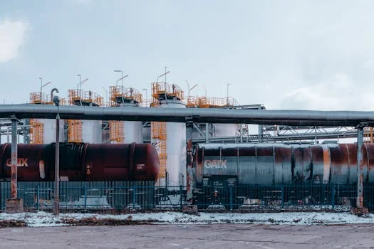
Forward Osmosis-Nanofiltration (FO-NF) hybrid systems reach 99% total water recovery at 8 to 10 kWh/m³, lower than thermal-heavy designs, but the entry price runs about $3.2 million for a 5 MGD train. They are tuned for 7 nm and 5 nm node fabs where HF and H₂SO₄ loads are high, and the modular skid cuts the physical footprint by roughly 30% versus RO-MVR, which matters during brownfield retrofits in crowded fab shells.
Reverse Osmosis-Mechanical Vapor Recompression (RO-MVR) systems price lower at about $2.5 million for a 5 MGD stream, but OPEX runs around $1.10 to $1.80/m³ because evaporation is energy-hungry. RO-MVR is usually the right pick for legacy fabs or sites handling high-TDS brines without extreme acid swings. RO membranes need replacement every 3 to 5 years; MVR evaporators require annual mechanical cleaning and descaling to keep heat transfer coefficients from drifting.
Pick based on the waste profile and the fab's energy tariff. FO-NF wins where electricity is expensive and recovery targets are aggressive. RO-MVR is the robust answer for diverse brine streams when the site can use existing steam or cheap power. Pairing HF wastewater treatment solutions for ZLD systems into either hybrid framework keeps fluoride below permit levels before the brine hits the crystallizer.
For a second design reference, Wafer Fab Wastewater ZLD: 2026 Engineering Specs, Hybrid System Design covers the same membrane-plus-thermal integration problem from a wafer-fab sizing angle. When chromium loading changes the pretreatment basis, start from Chip Fab Chromium Wastewater Treatment: 2026 Engineering Specs, ZLD Co instead.
| Metric | FO-NF Hybrid System | RO-MVR System |
|---|---|---|
| CAPEX (5 MGD) | $3.2M – $3.8M | $2.5M – $3.0M |
| OPEX (per m³) | $0.85 – $1.15 | $1.10 – $1.80 |
| Energy Consumption | 8 – 10 kWh/m³ | 12 – 15 kWh/m³ |
| Footprint | Compact (Modular) | Large (Thermal Skid) |
| Primary Use Case | Acidic/HF Streams (Advanced Nodes) | High TDS Brines (Legacy Fabs) |
Request every bid on a common basis: feed flow, peak flow, pH, fluoride, sulfate, silica, TDS, recovery definition, tariffs, cleaning downtime, and solids disposal. Without those fields, a lower CAPEX quotation can simply be omitting equalization, polishing, standby capacity, or disposal equipment.
What Does a Semiconductor ZLD System Cost and How Fast Is the ROI?
Capital expenditures for semiconductor ZLD systems run from $2.5 million for a small pilot to over $40 million for a 20 MGD campus-wide install, depending on how membrane and thermal stages are stacked. FO-NF systems carry a 20% to 30% CAPEX premium because forward osmosis membranes and draw-solution recovery units are specialty items, but OPEX lands at $0.85 to $1.50/m³ versus $1.10 to $1.80/m³ for RO-MVR (Saltworks 2024 data). Those OPEX figures bundle energy, antiscalant and cleaning chemical dosing, and scheduled membrane replacement.
Regional water stress drives the ROI. In water-stressed regions like Arizona or Taiwan, fabs typically hit payback in 3 to 5 years because they avoid freshwater procurement and brine disposal fees. In water-rich regions like Oregon, payback can stretch to 7 to 10 years, though ZLD is still often required to hold a discharge permit.
Procurement should budget lifecycle cost, not sticker price, and that includes the integration of RO systems for semiconductor water recovery plus the pretreatment chain ahead of them. For the full financial picture, engineers can reference detailed cost breakdowns for chip fab wastewater treatment to defend the higher CAPEX of high-efficiency hybrid trains against the long-term OPEX and compliance risk of a cheaper thermal-only line.
| Fab Capacity (MGD) | Estimated CAPEX (ZLD) | Annual OPEX (Avg) | ROI (Water-Stressed) |
|---|---|---|---|
| 5 MGD | $2.5M – $5.5M | $1.6M – $2.2M | 3.5 Years |
| 10 MGD | $12M – $18M | $3.5M – $4.8M | 4.2 Years |
| 20 MGD | $30M – $45M | $7.2M – $9.5M | 5.0 Years |
Use cost per MGD only after normalizing scope. A 5 MGD pilot with temporary utilities can cost more per unit of capacity than a 20 MGD campus system, while a brownfield retrofit can need more civil and electrical work than a greenfield train of the same flow. Separate direct equipment from tanks, foundations, electrical service, chemical storage, commissioning, and solids logistics before comparing bids.
Brine Disposal Cost Arizona Semiconductor Fab Projects: How to Model It
Brine disposal cost for an Arizona semiconductor fab starts at the screening range of $0.10 to $0.30 per gallon for high-TDS brine in the American Southwest, then gets replaced by written quotes. The model must carry charge per gallon, solids moisture, haul distance, acceptance limits, manifesting, and contingency capacity. Most plants we size for treat disposal as a reliability constraint, because one rejected load can stop a crystallizer discharge sequence.
Arizona project teams should test at least three routes: permitted liquid brine handling, evaporation and crystallization followed by solid disposal, and a qualified off-site treatment or injection route where legally available. Each route carries a different duty, outage exposure, sampling requirement, and long-term contract risk.
The decision changes when the brine becomes a solid. A filter press that produces 35–50% cake solids cuts haul volume, but the receiving facility may apply acceptance limits to fluoride, metals, organics, moisture, or leachability. The ZLD mass balance should show rejected salts and water separately so the disposal contractor can price the actual material.
Which IEEE/IPC Standards Govern ZLD Compliance at Chip Fabs?

IEEE 2030.1 standards for semiconductor manufacturing require ZLD systems to hold final discharge TDS below 50 mg/L, which forces high-rejection membrane processes plus thermal polishing on every train. The 2025 update to IPC-1758 requires new greenfield fabs to hit a minimum of 95% water recovery across the full site. Those standards exist because rapid fab expansion would otherwise drain local aquifers and push brine loads past what municipal wastewater infrastructure can absorb.
Sustainability rules under the CHIPS Act require fabs to cut freshwater intake by at least 20% by 2030 to stay eligible for certain federal incentives (DOE 2024). Beyond bulk water recovery, ZLD systems are now expected to remove emerging contaminants. Modern ZLD architectures must achieve 99.9% removal of PFAS (per- and polyfluoroalkyl substances) at the discharge point, alongside the existing TDS and heavy-metal limits that IEEE and IPC rules already enforce.
The compliance basis should separate a voluntary engineering target from a permit limit. The site owner should hold the current permit, sewer-use ordinance, pretreatment limits, stormwater requirements, hazardous-waste classification, and acceptance criteria for crystallizer solids. EPA's Section 309 authority confirms that permit and pretreatment violations can support federal enforcement, so those documents define the real design envelope.
Section 48D is a tax-credit issue, not a discharge standard. According to current IRS guidance, the advanced manufacturing investment credit equals 25% of qualified investment for property placed in service through December 31, 2025, and 35% for qualified property placed in service thereafter, with eligibility tied to facilities whose primary purpose is semiconductor manufacturing. The increase to 35% came from the Working Families Tax Cuts Act of 2025, so check the placed-in-service date and Form 3468 before booking the credit in an ROI model.
Who Should Choose FO-NF and Who Should Stay with RO-MVR?
FO-NF is the right pick for fabs on advanced nodes (7 nm and 5 nm) where HF and H₂SO₄ streams dominate, electricity costs run high, and the brownfield footprint is tight. RO-MVR fits legacy fabs, sites with diverse high-TDS brine but lower acid loading, and any plant that already has steam or low-cost power to feed the evaporator. In water-rich regions the OPEX gap narrows, so a CAPEX-driven RO-MVR bid often wins on simple payback.
Engineers procuring semiconductor ZLD systems should walk through a short checklist before signing: confirm the waste stream profile (HF, H₂SO₄, backgrind, scrubber blowdown), verify local water and discharge tariffs, confirm the available skid footprint, lock in the recovery target (95% per IPC-1758 for greenfield), and pressure-test Section 48D credit eligibility at 25% of qualifying spend through 2025 (35% thereafter). Most plants we size for in Arizona and Taiwan run at the lower end of the OPEX ranges above, because their feed water is already expensive.
Also confirm the operating envelope before award: minimum and maximum flow, equalization volume, clean-in-place frequency, crystallizer turndown, solids moisture, spare-parts lead time, and the bypass route used during a planned shutdown. Those details decide whether the design stays stable through fab ramp-up.
Send your feed-water analysis and target recovery rate, and we will size a ZLD train with CAPEX, OPEX, and ROI matched to your site. Request a semiconductor ZLD engineering quote with your daily flow and discharge limits.
Frequently Asked Questions
What is chip fab wastewater ZLD and why is it required?
Chip fab wastewater ZLD is a treatment train that recovers nearly all process water, up to 99% of it, and converts residual brine into a dry solid. It is required because fabs discharge 5 to 10 MGD of wastewater with TDS above 10,000 mg/L, which exceeds the capacity of municipal WRRFs and triggers IEEE 2030.1, IPC-1758, and CHIPS Act sustainability mandates. Earlier summaries cited $500,000 per year in penalties; EPA now sets Clean Water Act judicial civil penalties at up to $68,445 per day under 33 U.S.C. 1319(d).
How much does a semiconductor ZLD system cost in 2026?
CAPEX for a semiconductor ZLD system in 2026 ranges from $2.5 million for a 5 MGD pilot to over $40 million for a 20 MGD campus-wide install. OPEX runs $0.85 to $1.80 per cubic meter depending on whether the train is FO-NF or RO-MVR. According to IRS guidance, the Section 48D credit is 25% of qualified investment through December 31, 2025 and 35% thereafter. ROI lands between 3 and 5 years in water-stressed regions and 7 to 10 years in water-rich areas.
What is the difference between FO-NF and RO-MVR for chip fab ZLD?
FO-NF hybrids reach 99% water recovery at 8 to 10 kWh/m³ with a 30% smaller footprint, priced around $3.2 to $3.8 million for 5 MGD. RO-MVR systems price lower at $2.5 to $3.0 million for 5 MGD but consume 12 to 15 kWh/m³ because the MVR stage is thermal. FO-NF suits advanced-node HF/H₂SO₄ streams; RO-MVR suits legacy fabs with high-TDS brine and access to cheap steam or power.
Which IEEE and IPC standards apply to semiconductor wastewater ZLD?
IEEE 2030.1 sets the final discharge TDS limit at less than 50 mg/L for semiconductor manufacturing, and the 2025 update to IPC-1758 requires new greenfield fabs to achieve at least 95% water recovery. CHIPS Act rules layered on top require at least a 20% reduction in freshwater intake by 2030 to maintain eligibility for certain federal incentives. Together, those documents define the recovery, TDS, and intake targets that any ZLD design must hit.
How much energy does a chip fab ZLD system use per cubic meter?
FO-NF hybrid trains run at 8 to 10 kWh/m³ of permeate produced, while RO-MVR systems run at 12 to 15 kWh/m³ because the MVR crystallizer carries the bulk of the load. A 10 MGD fab with FO-NF and 99% recovery consumes roughly 1.4 to 1.8 MW of continuous electrical load, before pretreatment and pumping. Choosing the right train matters most where electricity costs exceed $0.08 per kWh.