Why Integrated Circuit Wastewater Treatment Costs Are Opaque (And How to Fix It)
Integrated circuit (IC) wastewater treatment systems for semiconductor fabs cost between $50,000 and $290,000 per unit (CAPEX), with OPEX ranging from $0.36 to $1.25 per cubic meter treated. Costs vary by flow rate (1–50 m³/h), contaminant load (fluoride, heavy metals, TOC), and treatment technology (MBR, DAF, RO). For a 10 m³/h system, expect $120,000–$250,000 CAPEX and $0.50–$0.90/m³ OPEX, with ROI achievable in 3–5 years via water reuse (up to 92% recovery).
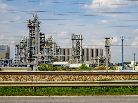
Semiconductor wastewater contains a complex cocktail of contaminants including fluoride, arsenic, copper, and high-load Total Organic Carbon (TOC), which requires a multi-stage engineering approach far beyond generic industrial filtration. While a standard manufacturing plant might deal with suspended solids, a single wafer fab can utilize tens of millions of gallons of water per day, resulting in high-volume streams that must meet stringent environmental discharge limits. The lack of transparent integrated circuit wastewater treatment price data often stems from the fact that no two fabs have the same chemical profile. For example, a facility focused on 28nm nodes will have a significantly different effluent profile than a legacy 200mm power semiconductor plant.
Current market data often provides a broad CAPEX range of $50,000 to $500,000, but these figures frequently omit the 20% to 40% in hidden costs associated with pre-treatment and sludge management. A 20 m³/h system designed specifically for fluoride removal may require an additional $30,000 per year in chemical dosing and pH adjustment alone. To fix the pricing opacity, procurement teams must evaluate the semiconductor wastewater treatment cost through the lens of contaminant concentration and desired recovery rates rather than simple flow volume. (Zhongsheng field data, 2025).
CAPEX Breakdown: What Drives Integrated Circuit Wastewater Treatment Prices?
Core treatment technologies account for 60% of the total CAPEX, with the remaining 40% allocated to automation, chemical feed systems, and civil engineering. For semiconductor facilities, the choice between Membrane Bioreactor (MBR), Dissolved Air Flotation (DAF), and Reverse Osmosis (RO) is the primary determinant of the initial investment. MBR systems for semiconductor wastewater typically range from $80,000 to $250,000 for capacities of 1–50 m³/h, offering 99% Total Suspended Solids (TSS) removal and high-quality effluent suitable for secondary reuse applications like cooling towers.
In contrast, DAF systems for pre-treatment in semiconductor fabs are more cost-effective for high-flow requirements (4–300 m³/h), costing between $50,000 and $150,000. While DAF is highly efficient at removing fats, oils, and greases (95% efficiency), it lacks the filtration fineness required for direct water reuse without subsequent stages. For fabs targeting ultra-pure water (UPW) recovery or Zero Liquid Discharge (ZLD), RO systems for water reuse in semiconductor manufacturing represent the highest tier of CAPEX, ranging from $120,000 to $290,000 for 10–200 m³/h configurations, but they provide the 95% recovery rates necessary for modern sustainability mandates.
Pre-treatment modules add a necessary layer of cost that engineers often overlook during the initial budgeting phase. pH adjustment skids ($5,000–$20,000), automated chemical dosing ($10,000–$30,000), and mechanical screening ($8,000–$25,000) are essential for protecting downstream membranes from the aggressive chemistries used in wafer etching and CMP (Chemical Mechanical Planarization). footprint requirements influence cost; underground integrated systems, such as the WSZ series, save valuable fab floor space but can add $20,000 to $50,000 in excavation and structural reinforcement costs. A 30 m³/h MBR system typically requires a 50 m² footprint compared to 80 m² for conventional A/O (Anaerobic/Oxic) systems. (Zhongsheng Engineering Specs, 2025).
| Technology Type | Flow Rate Capacity (m³/h) | Typical CAPEX Range (USD) | Primary Contaminant Focus |
|---|---|---|---|
| Dissolved Air Flotation (DAF) | 4 – 300 | $50,000 – $150,000 | Suspended Solids, FOG |
| Membrane Bioreactor (MBR) | 1 – 50 | $80,000 – $250,000 | TOC, TSS, Nitrogen |
| Reverse Osmosis (RO) | 10 – 200 | $120,000 – $290,000 | Dissolved Solids, Fluoride |
| Integrated WSZ (Underground) | 1 – 20 | $70,000 – $180,000 | Space-constrained BOD/TSS |
OPEX Deep Dive: The Hidden Costs of Treating Semiconductor Wastewater
Operational expenditures for semiconductor wastewater treatment are dominated by energy consumption and chemical reagents, which can fluctuate based on the wafer fab wastewater OPEX profile of the specific production node. Energy intensity varies significantly by technology: MBR systems consume 0.8–1.5 kWh/m³, DAF systems are lower at 0.3–0.6 kWh/m³, and RO systems for high-pressure desalination or reuse require 1.5–3.0 kWh/m³. For a fab operating 24/7, these energy requirements constitute 30% of the annual OPEX.
Chemical costs are particularly sensitive to fluoride removal in IC wastewater requirements. Treating high concentrations of fluoride (e.g., from hydrofluoric acid etching) typically requires calcium chloride or specialized coagulants, adding $0.10–$0.30/m³ to the treatment cost. Heavy metal precipitation (copper, nickel) adds another $0.05–$0.20/m³. A 20 m³/h system treating an average of 50 mg/L of fluoride can expect an annual chemical spend of $12,000 to $36,000. These costs are exacerbated by the need for pH stabilization using caustic soda or sulfuric acid, which is essential to meet local discharge permits.
Maintenance and consumables represent the "long tail" of the integrated circuit wastewater treatment price. MBR membranes have a service life of 3–5 years, with replacement costs ranging from $15,000 to $50,000 depending on the total surface area. RO membranes typically last 2–4 years and cost $20,000 to $80,000 per set. Sludge management is another critical factor; dewatered sludge with 20–30% solids must often be handled as hazardous waste in the semiconductor industry, costing $50–$150 per ton for disposal. Utilizing a plate and frame filter press can reduce volume and disposal costs by up to 60%, but the labor for operation must be factored into the $30,000–$60,000 annual labor budget for a dedicated EHS technician.
| OPEX Category | Estimated Cost per m³ | Annual Impact (10 m³/h System) | Key Driver |
|---|---|---|---|
| Energy Consumption | $0.15 – $0.45 | $13,000 – $39,000 | System Pressure / Aeration |
| Chemical Dosing | $0.10 – $0.50 | $8,700 – $43,800 | Fluoride & Metal Loads |
| Membrane Replacement | $0.08 – $0.20 | $7,000 – $17,500 | Flux Rate & Cleaning Cycles |
| Sludge Disposal | $0.05 – $0.15 | $4,300 – $13,100 | Hazardous Waste Levies |
| Labor & Monitoring | $0.20 – $0.40 | $17,500 – $35,000 | Automation Level |
ROI Calculator: How Water Reuse Cuts Integrated Circuit Wastewater Costs
Water reuse in semiconductor manufacturing can achieve recovery rates of 60% to 92%, drastically reducing the integrated circuit wastewater treatment price when viewed over a 10-year lifecycle. In semiconductor hubs like Taiwan, Singapore, or Arizona, where freshwater intake costs range from $0.50 to $2.00 per cubic meter, the ability to reclaim process water for cooling towers or scrubber make-up provides a direct hedge against rising utility prices. The ROI for wastewater treatment systems is calculated as: (Annual Water Savings + Compliance Fine Avoidance) / (Total CAPEX + Annual OPEX).
For instance, a 30 m³/h system achieving 80% water reuse saves approximately 210,000 cubic meters of freshwater annually. At a conservative rate of $1.00/m³, this results in $210,000 in annual savings. When combined with the avoidance of potential environmental fines—which can range from $10,000 to $100,000 per violation for exceeding fluoride or copper limits—the payback period often falls between 3 and 4 years. A pilot experiment in a Taiwanese fab recently demonstrated that a 92.3% reuse rate is technically feasible, effectively decoupling fab expansion from local water scarcity constraints.
Compliance benefits also include intangible but critical financial factors, such as accelerated permitting for facility expansions. In Singapore, fabs that implement ZLD (Zero Liquid Discharge) or high-recovery systems have historically reduced permit approval delays by up to 6 months compared to facilities relying on traditional discharge methods. This "time-to-market" advantage for new chip architectures can be worth millions in additional revenue, far outweighing the initial semiconductor wastewater treatment cost.
| Reuse Rate | Annual Water Savings (m³) | Annual Financial Return | Estimated ROI (Years) |
|---|---|---|---|
| 60% Recovery | 52,560 | $52,560 | 5.5 – 7.0 |
| 80% Recovery | 70,080 | $70,080 | 3.5 – 4.5 |
| 92% Recovery | 80,592 | $80,592 | 2.8 – 3.5 |
For more detailed calculations, consult our detailed CAPEX and OPEX breakdown for IC wastewater and use the engineering specs for semiconductor water reclaim to match your specific fab's parameters.
How to Choose the Right Integrated Circuit Wastewater Treatment System
Selecting the optimal system requires a decision framework that balances contaminant removal efficiency with long-term budget constraints. If your primary concern is fluoride removal in IC wastewater at high concentrations, a combination of chemical precipitation followed by an RO system for water reuse is the industry standard. RO can remove up to 99% of dissolved fluoride, though the pre-treatment stage is critical to prevent membrane scaling from calcium precipitates.
For fabs dealing with high organic loads and heavy metals (such as copper or nickel from plating processes), an MBR system integrated with an automatic chemical dosing system provides the most robust solution. MBR systems achieve 95% removal of heavy metals when paired with appropriate chelating agents. If the budget is constrained (under $100,000) and the goal is simple compliance for TSS and FOG before municipal discharge, a DAF system is the most scalable and cost-effective choice.
The following decision matrix helps engineers match technology to fab-specific needs:
| If your primary goal is... | And your budget is... | The recommended tech is... | Removal Efficiency |
|---|---|---|---|
| High Water Reuse (>85%) | High ($200k+) | RO + Advanced Oxidation | 99% TOC/TDS |
| Space Saving / Compliance | Mid ($120k-$200k) | MBR (Integrated) | 98% BOD/TSS |
| Pre-treatment / FOG removal | Low (<$100k) | DAF Machine | 95% TSS/FOG |
| Heavy Metal Sequestration | Mid ($100k-$180k) | Chemical Dosing + MBR | 95% Cu/Ni/As |
For engineers designing new facilities, reviewing an engineering guide for chip fab wastewater projects is essential to ensure that the integrated circuit wastewater treatment price quoted includes all necessary automation and compliance monitoring equipment.
Frequently Asked Questions
What is the typical payback period for an integrated circuit wastewater treatment system?
The payback period typically ranges from 3 to 5 years for systems designed with 60–80% water reuse. For more complex Zero Liquid Discharge (ZLD) systems, the ROI may extend to 5–7 years, though these are often justified by the ability to expand production in water-stressed regions where new freshwater permits are unavailable.
How does fluoride removal affect integrated circuit wastewater treatment costs?
Fluoride removal is a significant cost driver, adding $0.10–$0.30 per cubic meter in chemical costs (such as calcium chloride and polymers). It also requires specialized CAPEX investment in chemical reaction tanks and clarifiers, which can add $10,000–$30,000 to the initial system price compared to standard industrial filtration.
What are the compliance risks of not treating semiconductor wastewater?
Failure to meet discharge standards can result in fines ranging from $10,000 to $100,000 per violation, depending on the jurisdiction (EPA or local equivalent). Beyond financial penalties, fabs face the risk of permit revocation, which can halt production entirely. For example, a fab in California recently faced $250,000 in fines for repeated fluoride exceedances before upgrading their treatment infrastructure.
Can integrated circuit wastewater be reused in semiconductor manufacturing?
Yes, up to 92% of wastewater can be recovered using advanced RO or MBR technologies. While this water is often reused for non-critical processes like cooling towers or scrubbers, it can be polished to Ultra-Pure Water (UPW) standards using electrodeionization (EDI) and UV sterilization for use in the actual wafer fabrication process. A fab in Arizona currently reuses 70% of its effluent specifically for cooling tower make-up.
What are the maintenance requirements for an MBR system in a semiconductor fab?
MBR maintenance requires monthly membrane cleaning (CIP), quarterly calibration of chemical dosing pumps, and annual inspections of the aeration system. On average, a 20 m³/h MBR system requires approximately 4 hours of dedicated maintenance per month. Using a high-quality MBR module can extend the interval between deep cleans and reduce long-term OPEX.
Related Equipment
The following Zhongsheng Environmental products are engineered for the wastewater challenges discussed above:
- MBR systems for semiconductor wastewater — view specifications, capacity range, and technical data
- DAF systems for pre-treatment in semiconductor fabs — view specifications, capacity range, and technical data
Need a customized solution? Request a free quote with your specific flow rate and pollutant parameters.