Semiconductor fabs consume 5–10 million gallons of freshwater daily, with 38% of US sites in high-water-stress regions (WRI Aqueduct 2024). Water reuse systems can recover 60–95% of wastewater, reducing freshwater intake and discharge costs. Key contaminants—total dissolved solids (TDS), heavy metals (Cu, Ni, As), and fluoride—require advanced treatment like MBR (99% TSS removal) or RO (95% TDS rejection). Zero-liquid-discharge (ZLD) systems, combining forward osmosis (FO) and nanofiltration (NF), achieve 99% water recovery but at 3–5x the CAPEX of reuse systems. This guide provides 2025 engineering specs, recovery rates, and a decision framework to select the optimal system for your fab’s water footprint and budget.
Why Chip Fabs Must Prioritize Water Reuse: 2025 Water Stress and Regulatory Pressures
Semiconductor manufacturing facilities in the United States currently face a reality where 38% of existing and announced sites are located in high or extremely high water-stress regions, according to the 2024 WRI Aqueduct report. In regions like Phoenix, Arizona, and Austin, Texas, the competition for municipal water resources between industrial growth and residential demand has reached a critical inflection point. For fab facility engineers, the risk is no longer just a matter of corporate social responsibility; it is a matter of operational continuity. If a municipality cannot guarantee the 5–10 million gallons per day (MGD) required for a modern fab campus, production expansion becomes impossible.
Regulatory pressures are also tightening. By 2025, discharge limits for Total Suspended Solids (TSS) are expected to drop below 10 mg/L, while Chemical Oxygen Demand (COD) limits are trending toward <50 mg/L in sensitive watersheds. Heavy metal limits are even more stringent, with Copper (Cu) often capped at <0.5 mg/L and Nickel (Ni) at <0.1 mg/L under EPA guidelines and the EU Industrial Emissions Directive. In California and Arizona, local permits are increasingly requiring fabs to demonstrate a "net-zero" impact on local aquifers, effectively mandating aggressive water reuse or ZLD strategies.
The economic driver for chip fab wastewater water reuse is the escalating cost of municipal water and sewer services. In high-stress hubs, rates are rising 5–10% annually. For example, a fab in Phoenix pays approximately $5.20 per 1,000 gallons for combined water and sewer, whereas a site in Oregon may pay only $1.80. This disparity directly impacts the ROI of treatment infrastructure. Major players like Intel, Samsung, and TSMC have already pledged to reduce freshwater consumption by 30–50% by 2030 to meet ESG goals and mitigate these rising costs (Zhongsheng industry analysis, 2025).
| Fab Location | Water Stress Level | Estimated Water/Sewer Rate (per 1,000 gal) | 2025 Regulatory Trend |
|---|---|---|---|
| Phoenix, AZ | Extremely High | $5.20 | Mandatory Reuse / ZLD Incentives |
| Austin, TX | High | $4.85 | Strict Heavy Metal Limits (Cu <0.5 mg/L) |
| Dallas, TX | High | $4.10 | TDS Discharge Penalties |
| Albuquerque, NM | Extremely High | $3.90 | Aquifer Recharge Requirements |
| Hillsboro, OR | Low-Medium | $1.80 | COD/TSS Compliance Focus |
Chip Fab Wastewater Characteristics: Contaminants, Concentrations, and Treatment Challenges
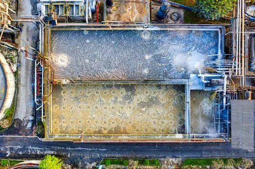
A state-of-the-art semiconductor fab produces distinct wastewater streams—CMP, etching, rinsing, and scrubber blowdown—each requiring specific pretreatment to manage high TDS and heavy metal concentrations. Chemical Mechanical Planarization (CMP) wastewater is particularly challenging due to its high concentration of nano-sized abrasive particles and dissolved metals, often reaching flow rates of 100–300 gpm with TDS levels between 500 and 2,000 mg/L. Etching and cleaning processes contribute significantly to fluoride and ammonia loads, which are difficult to remove through conventional biological treatment alone.
The primary engineering challenge in water reuse is the "concentration effect." As water is recovered, the remaining brine becomes increasingly concentrated with Total Dissolved Solids (TDS) and heavy metals. For instance, Copper (Cu) often forms stable complexes with organic acids used in the fab process, preventing standard precipitation. Similarly, Fluoride (F⁻) requires precise chemical dosing for semiconductor wastewater pretreatment to achieve precipitation at pH 10–11 using calcium hydroxide. Without effective heavy metal removal in semiconductor wastewater, these contaminants can foul downstream membranes or lead to permit violations.
| Contaminant | Typical Concentration (mg/L) | Source in Fab Process | Treatment Difficulty |
|---|---|---|---|
| TSS | 200–1,000 | CMP Slurry, Grinding | Low (Filtration/MBR) |
| COD | 100–500 | Solvents, Photoresist | Medium (Advanced Oxidation) |
| Copper (Cu) | 5–50 | CMP, Electroplating | High (Complexed ions) |
| Nickel (Ni) | 1–10 | Plating, Under-bump metallurgy | High (pH sensitivity) |
| Fluoride (F⁻) | 100–800 | Etching, Cleaning | Medium (Precipitation) |
| Ammonia (NH₄⁺) | 50–200 | Cleaning solutions | Medium (Stripping/Biological) |
| TDS | 500–2,500 | Blowdown, General process | High (Requires RO/ZLD) |
| TOC | 20–100 | Organics, IPA | Medium (Carbon/UV) |
| Arsenic (As) | 0.1–2.0 | Doping, Ion implantation | High (Strict limits) |
| Silica (SiO₂) | 50–150 | CMP slurry, Glass substrates | High (Membrane fouling) |
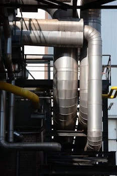
Water Reuse Technologies for Semiconductor Fabs: Engineering Specs and Recovery Rates
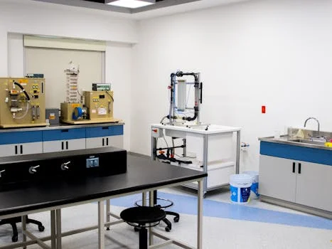
Advanced water reuse systems for chip fabs achieve recovery rates between 60% and 95% by integrating Membrane Bioreactors (MBR) and Reverse Osmosis (RO) with precision chemical dosing. MBR systems are particularly effective for treating combined streams with organic loads and suspended solids. For a 500 m³/day MBR system, engineering specifications typically demand submerged PVDF membranes with a flux rate of 15–25 Liters per Square Meter per Hour (LMH) and a pore size of 0.1 μm. This configuration ensures 99% removal of TSS and significant reduction in heavy metal-laden particles before the water reaches the RO stage.
Reverse Osmosis (RO) serves as the backbone of TDS removal. To prevent silica fouling—a common failure point in fab water reuse—systems must maintain a Silt Density Index (SDI) of <3 and utilize antiscalants such as polyacrylic acid. For brackish water applications, RO systems for semiconductor water reuse typically operate at 75–85% recovery. When higher recovery is required, Forward Osmosis (FO) and Nanofiltration (NF) hybrids are deployed. FO uses a draw solution to pull water through a semi-permeable membrane at low pressure, which significantly reduces energy consumption compared to high-pressure RO for high-TDS streams.
| Technology | Recovery Rate | TDS Rejection | Metal Removal | OPEX ($/1k gal) | Primary Limitation |
|---|---|---|---|---|---|
| MBR | 85–95% | N/A | >99% (Particulate) | $0.15–$0.30 | No dissolved salt removal |
| RO | 75–85% | 95–99.5% | >98% (Dissolved) | $0.40–$0.80 | Silica/Organic fouling |
| FO-NF Hybrid | 90–95% | >99% | >99% | $0.60–$1.20 | Draw solution management |
| DAF | 95% | N/A | 80–90% | $0.10–$0.20 | High chemical demand |
| Chem-Precip | N/A | N/A | >95% | $0.25–$0.50 | Sludge generation |
In a typical 500 m³/day MBR system for chip fab water reuse, the process flow begins with an equalization tank, followed by a fine screen (1mm). The water enters the aerobic tank where PVDF membranes are submerged. Air scours the membranes to prevent fouling while providing oxygen for biological degradation. The permeate is then pumped to an intermediate tank for pH adjustment before RO polishing. Energy consumption for this MBR stage typically ranges between 0.3 and 0.6 kWh/m³, making it a highly efficient pretreatment step for high-quality reuse (Zhongsheng field data, 2025).
Zero-Liquid-Discharge (ZLD) for Chip Fabs: When to Invest and How to Design the System
Zero-Liquid-Discharge (ZLD) systems eliminate liquid waste entirely by combining membrane concentration with thermal crystallization, though they require 3 to 5 times the capital investment of standard reuse systems. The decision to invest in ZLD is usually driven by one of three factors: extreme local water scarcity, total prohibition of liquid discharge into local sewers, or aggressive corporate ESG mandates for 99% water circularity. For a large fab in a region like Arizona, a ZLD system design for semiconductor fabs can save over $1 million annually in water and sewer fees, offsetting the high CAPEX over a 5-to-7-year period.
A standard ZLD architecture follows a four-stage process: Pretreatment (chemical softening/clarification), Membrane Concentration (High-Recovery RO or FO), Thermal Concentration (Brine Concentrator), and finally, Crystallization. The crystallizer is the most energy-intensive component, consuming 50–100 kWh/m³ of treated water. It uses evaporative technology to turn the final 1% of brine into dry salts—such as Sodium Chloride or Calcium Fluoride—which can sometimes be repurposed or sold. A 10M gallon/day fab utilizing an FO-NF-crystallizer hybrid can achieve 98-99% recovery, effectively closing the water loop.
| Decision Factor | Standard Water Reuse | Zero-Liquid-Discharge (ZLD) |
|---|---|---|
| Recovery Goal | 60–85% | 98–99.5% |
| CAPEX (1,000 gpm) | $3M – $6M | $12M – $25M |
| OPEX (per 1,000 gal) | $0.40 – $1.00 | $2.50 – $5.00 |
| Regulatory Driver | Discharge Compliance | No-Discharge Permit / Scarcity |
| Space Requirement | Moderate | High (Thermal footprint) |
Cost Breakdown and ROI Calculator for Chip Fab Water Reuse Systems
The capital expenditure (CAPEX) for a 1,000 gallon-per-minute (gpm) chip fab water reuse system typically ranges from $5 million to $10 million, depending on the complexity of the contaminant profile and desired recovery rate. Key cost drivers include the selection of membrane modules, the degree of automation required for 24/7 fab operations, and the civil works necessary for tankage and housing. A detailed cost breakdown for chip fab wastewater systems reveals that membrane replacement and energy consumption comprise nearly 60% of the long-term operational costs.
| System Size (gpm) | Estimated CAPEX Range | Annual OPEX (Estimated) | Primary Cost Driver |
|---|---|---|---|
| 100 gpm | $750,000 – $1.5M | $80,000 – $150,000 | Automation & Dosing |
| 500 gpm | $3M – $5M | $300,000 – $550,000 | Membrane Modules |
| 1,000 gpm | $6M – $11M | $650,000 – $1.2M | Energy & Pretreatment |
| 2,000 gpm | $12M – $20M | $1.5M – $2.5M | Civil Works & Footprint |
To calculate the ROI for a reuse system, facility managers should use the following formula: Payback (Years) = Total CAPEX / [(Annual Water Savings × Water Cost) + (Annual Discharge Savings × Sewer Rate) - Annual OPEX]. For example, a 500 gpm system in a high-cost region like Phoenix (CAPEX $3.5M, Water/Sewer $5.20/1k gal) achieving 80% recovery would save approximately $1.1M annually in water costs. After accounting for $400k in OPEX, the net annual savings of $700k results in a payback period of 5 years. Hidden costs to watch for include RO membrane fouling due to high silica (which can increase replacement frequency by 2x) and the scaling of crystallizers in ZLD configurations.
Frequently Asked Questions
What is the typical recovery rate for a semiconductor water reuse system?Standard water reuse systems for semiconductor fabs typically achieve recovery rates between 60% and 85%. By integrating advanced technologies like high-recovery RO or FO-NF hybrids, facilities can push these rates to 95%. True Zero-Liquid-Discharge (ZLD) systems reach 99% or higher by using thermal evaporation to eliminate the final brine stream. (Zhongsheng engineering data, 2025).
How do you handle high fluoride levels in fab wastewater?Fluoride is typically removed via chemical precipitation using calcium hydroxide (lime) or calcium chloride. By maintaining a pH of 10–11, fluoride reacts with calcium to form Calcium Fluoride (CaF₂) solids, which are then settled or filtered out. Typical dosing rates range from 100–300 mg/L of Ca(OH)₂ to reach discharge limits of <20 mg/L. (Per EPA 2024 wastewater guidelines).
What are the energy requirements for ZLD in a chip fab?ZLD is energy-intensive due to the thermal evaporation process. While standard RO reuse consumes 1.5–3 kWh/m³, a full ZLD system involving a crystallizer can consume 50–100 kWh/m³. Utilizing Mechanical Vapor Recompression (MVR) can lower these costs, but ZLD remains 10–20x more energy-intensive than basic filtration or MBR-based reuse.
Can reclaimed wastewater be used for Ultrapure Water (UPW) production?While technically possible, most fabs currently use reclaimed water for non-critical applications like cooling towers, scrubbers, and site irrigation to avoid risks to wafer yield. However, as treatment technologies like FO and advanced RO mature, a "closed-loop" back to the UPW system is becoming more common in water-scarce regions like Arizona and Taiwan. (WRI Aqueduct 2024 analysis).
What is the main cause of membrane fouling in fab wastewater?Silica (SiO₂) and organic photoresists are the primary foulants. Silica can precipitate on RO membranes if its concentration exceeds its solubility limit (typically ~120 mg/L at 25°C). Effective management requires specialized antiscalants, pH adjustment, or intermediate softening to ensure consistent membrane flux and lifespan.
Related Equipment
The following Zhongsheng Environmental products are engineered for the wastewater challenges discussed above:
- MBR systems for chip fab water reuse — view specifications, capacity range, and technical data
Need a customized solution? Request a free quote with your specific flow rate and pollutant parameters.