Semiconductor wastewater discharge standards in 2025 are among the strictest in manufacturing, with global limits tightening for fluoride (<10 mg/L in the EU, <15 mg/L in China), heavy metals (e.g., copper <0.5 mg/L in the US), and PFAS (70 ppt in the US, 0.1 μg/L in the EU). Fabs must now treat multiple streams—acid/alkaline, fluoride, CMP, and high-salinity wastewater—using tailored technologies like chemical precipitation, membrane systems, or Zero Liquid Discharge (ZLD). Compliance requires aligning treatment systems with regional regulations, water reuse targets, and emerging PFAS restrictions, with costs ranging from $2M–$15M for ZLD systems depending on fab size.
Why Semiconductor Wastewater Discharge Standards Are Unique
Semiconductor manufacturing generates at least six distinct contaminant streams—acids/alkalis, fluorides, heavy metals, Chemical Mechanical Polishing (CMP) slurries, organic solvents, and high-salinity brines—each requiring isolated treatment to prevent chemical interference. Unlike standard industrial effluent, fab wastewater contains ultrafine silica and ceria particles from CMP processes that are often smaller than 0.1 μm, rendering traditional sedimentation ineffective and necessitating advanced microfiltration or DAF systems for CMP wastewater pretreatment. the concentration of contaminants fluctuates significantly based on the production cycle, meaning a "one-size-fits-all" system will inevitably fail to meet 2025 compliance benchmarks.
The technical complexity is driven by the specific chemistry of wafer fabrication. For instance, the etching process utilizes hydrofluoric acid, resulting in fluoride concentrations that can exceed 1,000 mg/L in raw effluent. Meeting a 10 mg/L discharge limit requires high-precision precision chemical dosing for wastewater treatment compliance, typically involving two-stage calcium hydroxide precipitation at a controlled pH of 8.5 to 9.2. Organic solvents like Isopropyl Alcohol (IPA) further complicate matters by increasing Chemical Oxygen Demand (COD), often requiring Macro Porous Polymer Sorption (MPPS) or specialized biological treatment to meet municipal discharge requirements.
Regulatory challenges are compounding these technical hurdles. While Taiwan maintains a fluoride limit of 15 mg/L, the European Union’s Industrial Emissions Directive (IED) has pushed limits down to 10 mg/L for many regions. Additionally, the emergence of PFAS (per- and polyfluoroalkyl substances) as a regulated contaminant has introduced a new tier of treatment requirements. The US EPA’s Method 537.1 now targets limits as low as 70 ppt (parts per trillion), a threshold that standard wastewater plants are not equipped to reach without tertiary polishing stages like granular activated carbon or ion exchange.
Global Semiconductor Wastewater Discharge Standards 2025: A Region-by-Region Breakdown
Global semiconductor wastewater discharge standards for 2025 reflect a unified trend toward lower heavy metal thresholds and the first enforceable limits for "forever chemicals" like PFAS. Fab managers operating across multiple jurisdictions must navigate a patchwork of regulations where the strictest local limit often becomes the corporate engineering standard to ensure future-proofing. The following table consolidates current and upcoming limits across major semiconductor hubs.
| Region | Contaminant | Discharge Limit | Key Regulation | Compliance Deadline |
|---|---|---|---|---|
| United States | PFAS (PFOA/PFOS) Copper Fluoride |
70 ppt 0.5 mg/L 20 mg/L |
EPA NPDES / Clean Water Act | 2025-2026 (State dependent) |
| European Union | Fluoride Copper PFAS (Total) |
10 mg/L 0.5 mg/L 0.1 μg/L |
IED 2010/75/EU (BAT Conclusions) | Enforced (Ongoing) |
| China | Fluoride Ammonia Nitrogen Total Phosphorus |
15 mg/L 25 mg/L 1.0 mg/L |
GB 31573-2015 (Electronic Industry) | 2025 Update Pending |
| Taiwan | Fluoride Copper TSS |
15 mg/L 1.0 mg/L 30 mg/L |
EPA Effluent Standards | Enforced |
| South Korea | COD TSS Fluoride |
40 mg/L 10 mg/L 15 mg/L |
Water Environment Conservation Act | 2025 (New Fabs) |
In the US, the EPA is increasingly delegating PFAS enforcement to states like California and Arizona, where 70 ppt limits are becoming the standard for any fab discharging to sensitive groundwater basins. In the EU, the focus is on "Best Available Techniques" (BAT), which mandates not just the limit, but the specific technology class used to achieve it. China’s GB 31573-2015 remains the benchmark for the region, though localized standards in "Special Protection Areas" (like the Yangtze River Delta) often halve these limits for ammonia and phosphorus. For global operations, designing for the EU BAT standards typically ensures compliance across all other regions.
Treatment Technologies for Semiconductor Wastewater: How to Meet Discharge Standards
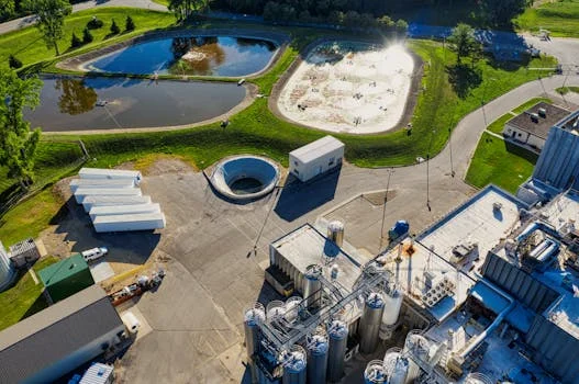
Effective treatment of semiconductor effluent requires a segregated approach where each waste stream is treated at the source before being combined for final polishing. For example, high-concentration fluoride streams must be isolated to prevent the formation of complexed metals that are harder to precipitate later. Modern fabs are increasingly turning to how industrial RO systems achieve 99.5% contaminant removal to handle high-salinity brines and enable water reuse. The table below outlines the primary technologies utilized to meet 2025 discharge standards.
| Contaminant Stream | Treatment Technology | Removal Efficiency | CAPEX Range | OPEX Range |
|---|---|---|---|---|
| Fluoride Waste | Two-stage Ca(OH)2 Precipitation | 95% - 98% | $500k - $2M | $0.80 - $1.50/m³ |
| CMP Wastewater | Electrocoagulation + UF | >99% TSS | $1M - $3M | $0.50 - $1.20/m³ |
| Heavy Metals (Cu, Ni) | Ion Exchange (IX) | >99.5% | $300k - $800k | $2.00 - $5.00/m³ |
| Organic Solvents | Advanced Oxidation (AOP) | 90% COD | $1M - $4M | $1.50 - $3.50/m³ |
| High-Salinity Brine | RO + Evaporation (ZLD) | 99.9% | $5M - $15M | $2.00 - $5.00/m³ |
| PFAS | GAC or Specialized Resins | >90% | $500k - $1.5M | $2.00 - $6.00/m³ |
To achieve fluoride limits below 10 mg/L, fabs use chemical dosing for fluoride and heavy metal precipitation with precise pH monitoring. If the limit is even lower (e.g., <2 mg/L for certain local reuse permits), tertiary treatment with activated alumina or specialized ion exchange resins is required. For CMP wastewater, the challenge is the stability of the colloidal silica; adding coagulants followed by ultrafiltration (UF) ensures that the effluent is clear enough for either discharge or as feed for RO systems for high-salinity wastewater treatment.
Zero Liquid Discharge (ZLD) vs. Water Reuse: Which System Meets Your Fab’s Needs?
The decision to implement a Zero Liquid Discharge (ZLD) system versus a partial water reuse system is primarily driven by local water scarcity and the stringency of discharge permits. In water-stressed regions like Arizona or Taiwan, ZLD is becoming a de facto requirement for new fabs. ZLD systems eliminate discharge risks entirely by converting wastewater into high-purity water for reuse and solid salt cakes for disposal. However, this comes at a significant cost premium compared to standard discharge or partial reuse systems. The decision matrix below helps evaluate these options based on 2025 economic and regulatory data.
| System Type | Water Recovery | CAPEX ($/m³) | Regulatory Benefit | Best Use Case |
|---|---|---|---|---|
| Standard Discharge | 0% | $1,500 - $3,000 | Low (Permit dependent) | Regions with abundant water |
| Partial Reuse | 70% - 85% | $4,000 - $7,000 | Moderate (Reduced volume) | Fabs with cooling tower demand |
| ZLD System | 95% - 98% | $12,000 - $25,000 | High (Zero permit risk) | Water-scarce or high-regulation zones |
A notable case study is TSMC’s adoption of ZLD in its advanced facilities, achieving over 95% water recovery. While the initial investment exceeded $10M, the ROI was realized within five years through reduced raw water procurement costs and the elimination of fluoride discharge fines. For fabs that do not require full ZLD, MBR systems for water reuse in semiconductor fabs offer a middle ground, treating organic-heavy streams for non-critical applications like cooling or scrubber make-up water. Detailed ZLD systems for semiconductor fabs: cost and performance data suggest that as discharge limits for PFAS and fluoride tighten, the "compliance gap" between standard treatment and ZLD is narrowing, making the latter more economically viable.
PFAS in Semiconductor Wastewater: Detection, Treatment, and Emerging Regulations

PFAS chemicals are integral to semiconductor manufacturing, found in photoresists, anti-reflective coatings, and specialized etching surfactants. According to the Semiconductor Industry Association (SIA) 2023 survey, PFAS concentrations in raw fab wastewater vary wildly, from low parts per billion (ppb) to high parts per trillion (ppt). Because these substances do not degrade naturally, 2025 regulations are shifting from monitoring to strict enforcement. Detection remains a primary hurdle; EPA Method 537.1 is the current standard for identifying 14-29 specific PFAS compounds, but many fabs are now being asked to test for "Total Organic Fluorine" (TOF) to capture the full spectrum of precursors.
Treatment of PFAS in the semiconductor context is typically handled at the "end-of-pipe" or after the primary fluoride removal stage. Granular Activated Carbon (GAC) is the most common technology, offering roughly 90% removal efficiency for long-chain PFAS like PFOA and PFOS. However, GAC is less effective for the short-chain PFAS often used in newer "green" photoresists. For these, high-affinity ion exchange (IX) resins or advanced oxidation processes (AOP) are required. While AOP can achieve >99% removal, its OPEX can reach $20/m³, making it a niche solution for highly concentrated streams. Intel’s PFAS reduction program, which invested over $5M in GAC and resin systems, serves as a benchmark for achieving 90%+ reduction in total discharge mass.
Compliance Checklist: How to Align Your Fab with 2025 Semiconductor Wastewater Standards
To ensure your facility remains compliant with the evolving 2025 semiconductor wastewater discharge standard, a systematic audit and upgrade path is required. Use the following checklist to evaluate your current treatment infrastructure:
- Stream Characterization: Conduct a full audit of all six major waste streams. Use ASTM D7979 or EPA 537.1 to establish a baseline for PFAS and fluoride concentrations.
- Gap Analysis: Compare baseline data against the 2025 regional limits (e.g., check if fluoride is <10 mg/L for EU sites or <15 mg/L for Asia-Pacific sites).
- Pretreatment Optimization: Ensure CMP wastewater is being treated with DAF systems for CMP wastewater pretreatment before mixing with other streams to prevent membrane fouling.
- Chemical Dosing Calibration: Verify that your chemical dosing for fluoride and heavy metal precipitation is utilizing dual-stage reaction tanks to hit the <10 mg/L target.
- Technology Selection: Evaluate if current RO or MBR systems need upgrading to High-Recovery RO (HRRO) to meet new water reuse mandates or ZLD requirements.
- PFAS Mitigation Plan: Install GAC or IX polishing stages if PFAS levels exceed 70 ppt. Plan for spent media disposal, as CERCLA designations may soon classify PFAS-laden carbon as hazardous waste.
- Real-time Monitoring: Implement online TOC (Total Organic Carbon) and fluoride analyzers to provide immediate alerts for process upsets that could lead to permit violations.
Frequently Asked Questions
What are the most stringent semiconductor wastewater discharge standards in 2025?
The European Union’s Industrial Emissions Directive (IED) sets the strictest limits for fluoride (<10 mg/L) and heavy metals (copper <0.5 mg/L). In terms of emerging contaminants, the US EPA’s 70 ppt limit for PFOA/PFOS represents the global benchmark for PFAS restriction.
How much does a ZLD system cost for a semiconductor fab?
For a mid-to-large scale fab, CAPEX for a ZLD system typically ranges from $5M to $15M. Operating expenses (OPEX) are between $2 and $5 per cubic meter of treated water. Most fabs in water-stressed regions see a payback period of 3 to 7 years through water savings and risk mitigation.
What treatment technology is best for removing PFAS from semiconductor wastewater?
Granular Activated Carbon (GAC) is the most cost-effective for long-chain PFAS (90% removal). For short-chain PFAS or stricter ppt-level compliance, specialized ion exchange resins or advanced oxidation processes (AOP) are required, though they carry higher OPEX.
Can semiconductor wastewater be reused in fab processes?
Yes. Using MBR systems for water reuse in semiconductor fabs combined with RO, wastewater can be reclaimed for cooling towers and scrubbers. With a full ZLD setup, the water can even be polished to Ultrapure Water (UPW) standards for wafer cleaning.
What are the penalties for non-compliance with semiconductor wastewater discharge standards?
Penalties include significant daily fines (up to $50,000/day in the US), mandatory production caps, and potential criminal liability for corporate officers. Beyond legal fines, non-compliance often results in the loss of "Green Fab" certifications, impacting ESG ratings and investor relations.