Why Semiconductor Fabs Lose Millions to Water Contamination
A semiconductor ultrapure water plant must hold resistivity >18.2 MΩ·cm at 25°C, TOC <1 ppb for critical organics, and silica <0.5 ppb. A 2024 300mm fab case linked a 12% defect rate to colloidal silica above 1 ppb in CMP (MKS Instruments, 2024). Makeup, primary, and polishing stages deliver that purity. CapEx for 1,000–3,000 m³/day plants is typically $1.2M–$4.5M.
Yield risk rises fast when wafer values exceed $10,000 each at 5nm and 3nm nodes. One 10nm particle can bridge circuit lines and create a killer defect. Residual organics can impair photoresist adhesion and shift line width across a lot. UPW demand also rises with wafer size: 300mm fabs often use about 3,000 m³/day, while 450mm concepts projected around 2027 have cited 5,000+ m³/day. Upstream wastewater control matters too; pretreatment for heavy metal removal in semiconductor wastewater lowers load on reclaim and makeup trains.
What Purity Limits Apply at 3nm and 5nm?
Advanced-node UPW at the point of distribution typically targets resistivity >18.2 MΩ·cm at 25°C, TOC at or below 1 ppb for critical organics, total silica ≤0.5 ppb, and particles <10 counts/mL above 0.05 μm. Earlier planning notes often cited the International Technology Roadmap for Semiconductors (ITRS) for a 2026 water use rate of 4.5 L/cm² of wafer. Buyers still use those volume figures for utility sizing, but the live yield roadmap is now the IEEE IRDS Yield Enhancement chapter.
According to ASTM D5127-13(2018), Type E-1.3 covers line widths of 0.065–0.032 μm at the point of distribution, with on-line resistivity 18.2 MΩ·cm, TOC 1 µg/L (ppb), and total silica 0.5 µg/L. Earlier wording referred to an "ASTM E-1.3" water standard; the correct designation is ASTM D5127 Type E-1.3 (ASTM, 2018). The 2024 IRDS Yield Enhancement chapter keeps immersion-lithography TOC <1.0 ppb as a point-of-use driver, while non-critical organics may be managed to <3 ppb and critical organics to <1 ppb (IEEE IRDS, 2024).
US and UK fabs apply the same POD chemistry targets. Local codes mainly affect discharge permits and reclaim rates, not the UPW purity table itself. Reliability and protection come from stage gating: primary effluent should reach TOC <5 ppb before polishing so the final loop is not overloaded by upstream organics or ions. Bacteria limits and dissolved nitrogen stability also appear in ASTM D5127 tables for electronic-grade water and should be copied into the project basis of design.
For procurement packages, state whether each limit applies at POD, POC, or POU. Immersion lithography often needs the tightest TOC at POU even when the distribution loop runs a slightly wider non-critical organic budget under IRDS. Write that split into the P&ID notes so vendors do not bid a single average TOC that fails the tool.
2026 Specs for a Semiconductor Ultrapure Water Plant
Semiconductor UPW plant architecture still rests on three stages: makeup (pretreatment), primary (TOC reduction and deionization), and polishing (ultrafiltration and degasification). Each stage has hard hand-off limits so defects are not pushed downstream. The table below keeps the same stage targets used for 2026 design reviews on advanced-node projects.
| Treatment Stage | Key Parameter | Target Specification (2026) | Primary Technology |
|---|---|---|---|
| Makeup (Pretreatment) | Turbidity | < 0.1 NTU | Multimedia Filtration, Cartridge Filtration |
| Hardness (as CaCO₃) | < 1 mg/L | Water Softening, RO | |
| Total Dissolved Solids (TDS) | < 50 ppm | RO | |
| Primary (TOC Reduction) | Resistivity | > 1 MΩ·cm | Mixed Bed Ion Exchange, CDI |
| Total Organic Carbon (TOC) | < 5 ppb (influent to Polishing) | UV Oxidation (185nm), CDI | |
| Conductivity | < 0.055 μS/cm | Mixed Bed Ion Exchange, CDI | |
| Polishing | Particles (>0.05 μm) | < 10 counts/mL | Ultrafiltration (UF) |
| Dissolved Oxygen (DO) | < 1 ppb | Membrane Degasification | |
| Silica (SiO₂) | < 0.5 ppb | Ion Exchange, RO |
These stage gates align with ASTM D5127 Type E-1.3 POD values for resistivity, TOC, and silica on the finest listed line widths. They also leave headroom for IRDS point-of-use TOC control on immersion tools. If feed water is high in hardness or organics, expand makeup before upsizing polishing resin or EDI modules.
Design reviews should freeze these stage targets in the URS before vendor kickoff. Changing TOC or silica limits after P&ID approval usually forces RO, UV, or polishing skid redesign and schedule slip. Keep a signed limits sheet with units and sample points attached to every RFQ.
Process Breakdown: How Each Stage Achieves 18.2 MΩ·cm Resistivity
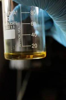
The makeup stage is the first barrier against bulk solids and salts. Multimedia filtration cuts turbidity to <0.1 NTU. Softening holds hardness below 1 mg/L as CaCO₃ to limit scale on RO membranes. Reverse osmosis then removes most salts and organics, often to TDS <50 ppm, so downstream ion exchange or CDI is not overloaded. On high-TOC surface water, add activated carbon or a second RO pass in makeup before relying on 185 nm UV alone.
Primary treatment does the TOC and resistivity work. UV at 185 nm oxidizes organics to CO₂ and water. Continuous electrodeionization (CDI/EDI) or mixed-bed ion exchange then strips residual ions. The usual hand-off is conductivity below 0.055 μS/cm and TOC under 5 ppb before polishing. An EDI Electrodeionization System is often selected when chemical-free regeneration and high recovery are priorities.
Polishing finishes particle and gas control. Filters at 0.05 μm capture sub-micron particles. Membrane degasification removes dissolved oxygen and nitrogen toward <1 ppb DO. Final UPW must meet <10 counts/mL for particles >0.05 μm. Failure modes matter in design reviews. CDI membranes foul when influent conductivity exceeds about 10 μS/cm. UF membranes fail under free chlorine. Reliable RO systems for semiconductor UPW pretreatment keep primary and polishing stages inside those limits.
CDI vs. Mixed Bed Ion Exchange: Cost, Efficiency, and Risk Trade-offs
Continuous electrodeionization (CDI) and mixed-bed ion exchange (IX) both support high resistivity after RO and UV. CDI OpEx is typically about 40% lower than mixed-bed IX because chemical regeneration is eliminated. Water recovery is about 95% for CDI versus about 85% for mixed-bed IX. Mixed-bed IX CapEx can start near $800,000, while CDI may require about $1.2 million for similar flow. Mixed-bed IX still tolerates influent conductivity up to about 20 μS/cm before regeneration, versus about 10 μS/cm for many CDI trains.
| Feature | CDI (Continuous Electrodeionization) | Mixed Bed Ion Exchange |
|---|---|---|
| CapEx | Higher ($1.2M+) | Lower ($800K+) |
| OpEx ($/m³) | Lower (estimated $0.10-$0.20) | Higher (estimated $0.20-$0.35) |
| Footprint | Generally more compact | Can be larger due to regeneration skid |
| Maintenance Frequency | Lower (no chemical regeneration) | Higher (resin replacement, chemical handling) |
| Water Recovery | ~95% | ~85% |
| Chemical Usage | None (for regeneration) | Acids and bases for regeneration |
| Waste Generation | Minimal (membranes, electrodes) | Spent resins (hazardous waste) |
| Influent Conductivity Tolerance | Lower (typically <10 μS/cm) | Higher (up to 20 μS/cm) |
| Compatibility with 3nm/5nm Fabs | High (with proper pretreatment) | Proven, High |
Pilot data on your RO permeate is worth more than generic recovery claims. Choose CDI when OpEx, chemical handling, and recovery dominate the decision and pretreatment is strong. Choose mixed-bed IX when CapEx is tight, influent conductivity swings are wider, or the fab already runs acid and caustic regeneration. chemical dosing for UPW pH adjustment and resin regeneration remains essential on IX trains and for loop pH control.
2026 CapEx/OpEx Models for Semiconductor UPW Plants
CapEx for UPW plants scales with capacity. A 1,000 m³/day train for R&D or pilot fabs often ranges from $1.2 million. High-volume 300mm fabs at about 3,000 m³/day can reach $4.5 million. Concepts for 450mm fabs at 5,000+ m³/day have been estimated at $6 million to $8 million CapEx.
OpEx is usually energy-heavy. About 50% of operating cost goes to power for RO and UV. Resin replacement is about 30% on mixed-bed systems. Membrane replacement for RO and UF is about 10%. Labor and chemicals are each about 5%. Unit cost of UPW is often $0.80–$1.20/m³ on CDI-based trains and $1.10–$1.50/m³ on mixed-bed IX trains under typical municipal feed quality.
Budget owners should separate installed CapEx from owner costs. Civil works, cleanroom piping in PVDF or similar, online analyzers, and spare EDI modules often sit outside the skid price. A bid that looks low at $2.5M for 3,000 m³/day can exceed $4.5M once distribution, monitoring, and commissioning are included. Ask for a scope matrix that lists every analyzer, valve, and resin charge.
| Fab Size/Capacity | Estimated CapEx | Estimated OpEx ($/m³) (CDI-based) | Estimated OpEx ($/m³) (Mixed Bed IX) | Annual Yield Loss Savings (3000 m³/day fab) |
|---|---|---|---|---|
| 1,000 m³/day (Small Fab/R&D) | $1.2M - $2.0M | $0.80 - $1.00 | $1.10 - $1.30 | N/A |
| 3,000 m³/day (300mm Fab) | $2.5M - $4.5M | $0.90 - $1.20 | $1.20 - $1.50 | ~$1.2M (vs. 5 ppb TOC system) |
| 5,000+ m³/day (450mm Fab) | $6.0M - $8.0M | $0.85 - $1.15 | $1.15 - $1.45 | ~$2.0M+ (vs. 5 ppb TOC system) |
A 3,000 m³/day plant that holds TOC below 1 ppb can save about $1.2 million per year versus a legacy 5 ppb TOC system through lower defect rates. compact UPW pretreatment systems for semiconductor fabs help lock influent quality before the high-purity stages.
How Do You Estimate 20-Year UPW Lifecycle Cost?
A 20-year UPW lifecycle cost is CapEx plus discounted OpEx for energy, membranes, resin or EDI modules, chemicals, labor, and waste disposal, minus yield-loss savings from meeting resistivity and TOC targets. Use the unit OpEx ranges above ($0.80–$1.50/m³) at the design daily volume. Then add membrane and resin change-outs on the OEM interval for your feed water.
For a 3,000 m³/day fab running 330 days/year, annual UPW volume is about 990,000 m³. At $1.00/m³ CDI OpEx that is roughly $0.99M/year before major replacements. Over 20 years, energy price escalation and resin or module swaps usually dominate. Technology choice between CDI and mixed-bed IX therefore matters more than small CapEx deltas. Fab wastewater and reclaim strategy also affect makeup volume. Compare wastewater treatment options for semiconductor fabs when modeling water balance and discharge fees.
Lifecycle models should also carry sensitivity cases for feed TDS, recovery, and alarm divert frequency. A plant that diverts 5% of polished flow on TOC spikes can erase much of the OpEx advantage of CDI. Build the model around measured feed data, not brochure recovery alone. Include disposal fees for spent mixed-bed resin as hazardous waste where local rules require it. CDI shifts cost toward module replacement, so enter the OEM membrane and electrode life in hours, not only calendar years.
Equipment Selection Checklist for Semiconductor Fabs
Match plant capacity to fab size first. Many 300mm lines need about 3,000 m³/day. Concepts that still use 450mm planning figures often cite 5,000+ m³/day. Next select TOC reduction: CDI or EDI for lower OpEx when RO permeate stays below about 10 μS/cm, or mixed-bed IX when influent swings are wider. Then set polishing: 0.05 μm UF plus membrane degasification for CMP and critical cleans. Filters at 0.1 μm may suffice on older nodes. Finally install continuous resistivity, TOC, and particle monitoring with hard alarms. For example, TOC above 1.5 ppb should trigger divert or shutdown. Document who owns the divert decision: facilities, process engineering, or the tool owner. Ambiguous ownership is a common root cause of contaminated wafers after night-shift alarms.
- Confirm design flow in m³/day against peak tool demand and reclaim contribution.
- Verify RO permeate conductivity before CDI or polishing mixed beds.
- Specify UV 185 nm dose and H₂O₂ control; IRDS cites a 3 ppb H₂O₂ target in UPW (IEEE IRDS, 2024).
- Require POD metrology for resistivity, TOC, silica, particles, and DO.
- Score CapEx, OpEx ($/m³), chemical handling, and hazardous waste before award.
- Document spare membranes, resin, and EDI modules for 24-month operation.
- Align alarm setpoints with fab yield engineering, not only vendor defaults.
For 3nm/5nm low-OpEx duty, use RO, UV, CDI, 0.05 μm UF, degas, and monitoring. For 3nm/5nm high-purity focus with wider feed swings, use RO, UV, mixed-bed IX, 0.05 μm UF, degas, and monitoring. Older nodes may use 0.1 μm UF. An EDI Electrodeionization System fits the low-OpEx stack when pretreatment is proven.
When comparing vendor proposals, normalize every quote to the same feed analysis, recovery, and POD limits. Otherwise a low CapEx bid may assume softer water or lower TOC than your well or river actually delivers. Require a water-balance diagram that shows concentrate, regenerate waste, and divert volumes in m³/day. Those streams drive sewer fees and often dominate OpEx after year three.
Commissioning should prove each stage gate with real instruments, not only factory acceptance data. Run turbidity, hardness, RO permeate conductivity, primary TOC, and polished resistivity for at least one stable production-like week. Record divert events and root causes before beneficial occupancy of the wet benches.
Who this is for: process engineers, EPC contractors, and procurement teams sizing or upgrading UPW for 300mm advanced-node fabs. Who should look elsewhere: labs that only need ASTM Type II or III reagent water, or plants without semiconductor particle and TOC specs. Next step: send feed-water analysis, design flow in m³/day, and node purity targets for a staged makeup–primary–polishing mass balance.
Frequently Asked Questions
What UPW resistivity and TOC do 3nm fabs need?
Most 3nm and 5nm lines specify resistivity >18.2 MΩ·cm at 25°C and TOC at or below 1 ppb for critical organics. ASTM D5127 Type E-1.3 lists TOC 1 µg/L and total silica 0.5 µg/L for 0.065–0.032 μm line widths. IRDS 2024 still treats immersion-lithography TOC <1.0 ppb as a POU driver while allowing non-critical organics up to <3 ppb in the broader water-quality table.
How much CapEx for a 3000 m3/day UPW plant?
Estimated CapEx for a 3,000 m³/day semiconductor UPW plant is $2.5M–$4.5M under the 2026 models in this article. Smaller 1,000 m³/day R&D plants sit near $1.2M–$2.0M. Larger 5,000+ m³/day concepts are modeled at $6.0M–$8.0M. Final quotes depend on feed quality, recovery target, CDI versus mixed-bed IX, and polishing loop design.
Is CDI or mixed-bed ion exchange better for UPW?
CDI usually wins on OpEx ($0.10–$0.20/m³ estimated) and about 95% recovery when RO permeate conductivity stays below about 10 μS/cm. Mixed-bed IX usually wins on CapEx from about $800K and tolerates influent conductivity up to about 20 μS/cm. Its OpEx rises to about $0.20–$0.35/m³ with chemicals and spent resin. Pick based on OpEx priority, chemical handling capacity, and pretreatment strength.
What causes UPW-related yield loss in CMP?
Colloidal silica, TOC, particles, and dissolved ions are the main UPW-linked CMP yield killers. A 2024 300mm fab case linked a 12% defect rate to colloidal silica above 1 ppb (MKS Instruments, 2024). Keep silica <0.5 ppb, particles <10 counts/mL above 0.05 μm, and DO <1 ppb at polishing. Divert on TOC alarms before tools see off-spec water.
Does UV 185 nm alone meet semiconductor TOC specs?
UV at 185 nm breaks down dissolved organics but does not replace ion exchange or CDI for resistivity, nor UF for particles. Use UV in the primary stage to drive TOC toward <5 ppb before polishing. Finish with mixed-bed or EDI polishing and membrane degasification. IRDS also flags H₂O₂ by-product from 185 nm UV, with a 3 ppb H₂O₂ target in the UPW roadmap (IEEE IRDS, 2024).
Related Equipment
- continuous electrodeionization stacks for UPW plants — UPW train designers can match polisher capacity to their RO permeate flow.