Semiconductor Nickel Wastewater Treatment: Engineering Specs, Recovery ROI & Equipment Selection 2025
Semiconductor fabs generate wastewater with nickel concentrations up to 500 mg/L from CMP, etching, and rinsing processes. Advanced treatment systems can recover 95%+ of water and 100% of nickel (e.g., Memsift’s 10.2 ton/year recovery case), reducing discharge violations and turning waste into revenue. Key technologies include reverse osmosis (RO) for high-purity permeate, electrocoagulation for chelate-free removal, and advanced oxidation processes (AOP) for organic-bound nickel. Compliance with EPA 40 CFR Part 469 or EU Directive 2010/75/EU requires effluent nickel levels below 0.1 mg/L—achievable with tailored equipment selection.Why Nickel Wastewater Treatment is a Critical Challenge for Semiconductor Fabs
Semiconductor manufacturing processes, including chemical mechanical polishing (CMP), etching, and various rinsing steps, are primary sources of nickel-contaminated wastewater, with concentrations ranging from 1 mg/L to over 500 mg/L. For instance, CMP slurries can contain 100–500 mg/L nickel, etching baths 50–200 mg/L, and rinsing steps 1–50 mg/L. This wastewater typically follows a process flow of CMP → rinse → wastewater collection → pretreatment → nickel recovery, necessitating robust treatment solutions to meet stringent regulatory limits and mitigate environmental and financial risks. Regulatory frameworks globally impose strict nickel effluent limits; the EPA 40 CFR Part 469 mandates a daily maximum of 0.1 mg/L Ni and a monthly average of 0.05 mg/L Ni for the semiconductor subcategory, while the EU Directive 2010/75/EU sets a limit of 0.2 mg/L. Asian regions often have even stricter local permits, such as Taiwan’s 0.05 mg/L and China’s GB 21900-2008 at 0.5 mg/L, underscoring the need for advanced treatment. The financial impact of unaddressed nickel wastewater is substantial, encompassing both lost revenue from unrecovered metal and significant penalties for non-compliance. With nickel market prices fluctuating between $20,000–$25,000/ton in 2025, the potential for recovery represents a considerable revenue stream; a notable case from Memsift demonstrated 10.2 tons/year of nickel recovery. Conversely, non-compliance can lead to severe financial repercussions, with EPA fines reaching up to $54,833 per day per violation. Beyond monetary penalties, environmental risks associated with nickel discharge are profound. Nickel is toxic to aquatic life, with an LC50 for *Daphnia magna* typically between 0.05–0.5 mg/L, and it exhibits bioaccumulation properties in sludge, posing long-term disposal challenges. public perception risks for fabs located near water bodies can negatively impact corporate reputation and social license to operate.Reverse Osmosis for Nickel Removal: Engineering Specs, Efficiency Data & Limitations
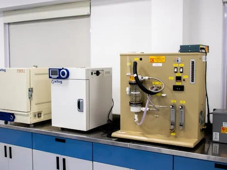
Table 1: Typical Nickel Removal Efficiency for RO Systems
| Influent Nickel Concentration (mg/L) | Target Effluent Nickel Concentration (mg/L) | Nickel Removal Efficiency (%) | Applicability |
|---|---|---|---|
| 200 (ionic) | < 0.1 | 99+ | High-purity water reuse, compliance |
| 50 (ionic) | < 0.05 | 99+ | Strict local limits |
| 100 (chelated) | 10-20 | 80-90 | Requires pretreatment for compliance |
Electrocoagulation: How It Breaks Nickel Chelates and Reduces Sludge Volume
Electrocoagulation (EC) effectively removes nickel from semiconductor wastewater, particularly excelling in breaking down challenging nickel chelate wastewater treatment complexes. The electrocoagulation process involves the electrochemical dissolution of a sacrificial anode (typically aluminum or iron) into the wastewater. This generates metal hydroxide flocs *in situ* which, alongside the production of hydroxyl radicals (·OH), effectively adsorb and precipitate ionic nickel while simultaneously breaking down chelating agents like EDTA or citrate. This mechanism allows EC to achieve 90–98% nickel removal efficiency for chelated nickel, significantly outperforming RO systems that typically manage 80–90% for such complexes. Lab-scale studies demonstrate effluent concentrations below 0.5 mg/L are achievable for chelated nickel streams. For a comprehensive understanding of the engineering mechanics and process flow, explore our article on electrocoagulation for heavy metal removal.Table 2: Nickel Removal Efficiency Comparison for Electrocoagulation
| Nickel Form | Influent Concentration (mg/L) | Effluent Concentration (mg/L) | Removal Efficiency (%) |
|---|---|---|---|
| Ionic Nickel (Ni²⁺) | 100 | < 0.1 | > 99 |
| Chelated Nickel (e.g., Ni-EDTA) | 50 | < 0.5 | 90-98 |
Advanced Oxidation Processes (AOP) for Nickel Wastewater: UV, Ozone, and Fenton’s Reagent
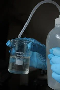
Table 3: Comparison of Common AOP Methods for Semiconductor Wastewater
| AOP Method | Primary Oxidant | Capital Cost (Relative) | OPEX (Relative) | Footprint (Relative) | Best For |
|---|---|---|---|---|---|
| UV/H₂O₂ | Hydroxyl radicals from H₂O₂ + UV | Medium | Medium (H₂O₂, UV lamps) | Medium | Organic ligand degradation, moderate COD |
| Ozone/H₂O₂ | Hydroxyl radicals from O₃ + H₂O₂ | High (ozone generator) | High (energy for O₃, H₂O₂) | Large | High COD, refractory organics |
| Fenton’s Reagent (Fe²⁺/H₂O₂) | Hydroxyl radicals from Fe²⁺ + H₂O₂ | Low | Medium (H₂O₂, Fe salts, pH adjust) | Small | Batch processes, high COD, requires pH adjustment |
Head-to-Head Comparison: RO vs. Electrocoagulation vs. AOP for Nickel Wastewater
Selecting the optimal nickel wastewater treatment technology for semiconductor fabs hinges on a nuanced understanding of influent characteristics, effluent goals, and operational economics. Each technology—Reverse Osmosis (RO), Electrocoagulation (EC), and Advanced Oxidation Processes (AOP)—offers distinct advantages and limitations. RO excels at achieving very low effluent nickel levels and high water recovery for reuse, but struggles with chelated nickel and is susceptible to fouling. Electrocoagulation is highly effective at breaking down nickel chelates and reducing sludge volume, making it ideal for complex semiconductor CMP wastewater. AOPs are paramount for oxidizing organic ligands that bind nickel, acting primarily as a pretreatment to enhance the performance of subsequent physical-chemical or membrane processes.Table 4: Head-to-Head Comparison of Nickel Wastewater Treatment Technologies
| Technology | Nickel Removal (%) | Effluent Ni (mg/L) | CAPEX ($/m³/day) | OPEX ($/m³) | Footprint (m²/m³/day) | Best For |
|---|---|---|---|---|---|---|
| Reverse Osmosis (RO) | 95-99 (ionic) | < 0.01 | $1,500-3,000 | $0.20-0.60 | 0.05-0.15 | High-purity water reuse, ionic nickel, polishing |
| Electrocoagulation (EC) | 90-98 (chelated) | < 0.5 | $800-2,000 | $0.30-0.70 | 0.03-0.10 | Chelated nickel, sludge reduction, pretreatment |
| Advanced Oxidation (AOP) | 80-95 (release) | (Pretreatment) | $1,000-2,500 | $0.25-0.80 | 0.04-0.12 | Organic-bound nickel, COD reduction, RO pretreatment |
Nickel Recovery ROI: CAPEX, OPEX, and Payback Period for Semiconductor Fabs
Table 5: Estimated CAPEX Ranges for Nickel Wastewater Treatment Systems (2025)
| Technology | 50 m³/day System CAPEX | 200 m³/day System CAPEX | 500 m³/day System CAPEX |
|---|---|---|---|
| Reverse Osmosis (RO) | $75,000 - $150,000 | $300,000 - $600,000 | $750,000 - $1,500,000 |
| Electrocoagulation (EC) | $40,000 - $100,000 | $160,000 - $400,000 | $400,000 - $1,000,000 |
| Advanced Oxidation (AOP) | $50,000 - $125,000 | $200,000 - $500,000 | $500,000 - $1,250,000 |
Equipment Selection Checklist: 7 Critical Questions for Semiconductor Nickel Wastewater Systems
Selecting the appropriate nickel wastewater treatment system for a semiconductor fab requires a systematic evaluation of several critical factors to ensure compliance, maximize recovery, and optimize operational efficiency. A structured approach helps engineers and procurement teams make informed decisions.- Influent Characteristics: What are the precise nickel concentrations (mg/L), is nickel predominantly chelated (yes/no), what are the typical pH and COD levels, and what is the average and peak flow rate (m³/day)? Understanding these parameters is foundational for system design.
- Effluent Requirements: What are the local discharge limits for nickel (mg/L)? Are there specific water reuse targets (%) for non-process applications (e.g., cooling towers, rinsing)? What are the regulations for nickel sludge disposal?
- Recovery Goals: What is the desired nickel recovery rate (%), and what is the target water recovery rate (%)? What is the projected annual revenue potential ($/year) from recovered nickel?
- Footprint Constraints: How much available space (m²) is there for the treatment system? Will it be an indoor or outdoor installation, and are modularity needs a consideration for future expansion?
- Budget: What is the allocated capital expenditure (CAPEX) for the system? What is the acceptable operational expenditure (OPEX) per cubic meter ($/m³), and what is the target payback period (years)?
- Integration: How will the new system integrate with existing pretreatment infrastructure, such as pH adjustment or multimedia filtration? Is it compatible with downstream systems like high-efficiency filter presses for nickel sludge dewatering? Consider PLC-controlled chemical dosing for nickel wastewater pretreatment for seamless integration.
- Vendor Support: What is the availability of local service and technical support? What are the lead times for spare parts, and are comprehensive training programs offered for plant operators?
Frequently Asked Questions
- Q: What is the most cost-effective technology for nickel wastewater with high COD?
A: Electrocoagulation or AOP + RO hybrids are most cost-effective for high-COD streams (COD > 500 mg/L), as RO alone suffers from fouling. Electrocoagulation reduces COD by 60–80% while removing nickel, while AOP breaks organic ligands to enable downstream RO. - Q: Can nickel wastewater be reused in semiconductor manufacturing?
A: Yes, but only after advanced treatment. RO permeate (nickel < 0.01 mg/L) can be reused for rinsing or cooling towers, while electrocoagulation effluent (nickel < 0.5 mg/L) may require further polishing for process water. Reuse typically requires a 2-stage RO or MBR system. - Q: What are the EPA’s nickel discharge limits for semiconductor fabs?
A: Under 40 CFR Part 469, the daily maximum is 0.1 mg/L Ni and the monthly average is 0.05 mg/L Ni for the semiconductor subcategory. Some states (e.g., California) have stricter limits (0.02 mg/L). Always check local permits. - Q: How do I reduce sludge volume from nickel precipitation?
A: Use electrocoagulation (30–50% less sludge than chemical precipitation) or a lamella clarifier for high-efficiency sedimentation. For existing systems, optimize coagulant dosage (e.g., polyaluminum chloride) and add a sludge thickener before dewatering. - Q: What pretreatment is needed for RO systems treating nickel wastewater?
A: Pretreatment typically includes pH adjustment (to 6–8), multimedia filtration (to remove TSS), and antiscalant dosing (to prevent silica fouling). For chelated nickel, AOP or electrocoagulation is required upstream of RO to prevent membrane fouling.