Why Third-Generation Semiconductor Developer Wastewater Demands Specialized Treatment
Third-generation semiconductor developer wastewater contains significantly higher concentrations of problematic contaminants compared to other fab streams, making conventional treatment methods insufficient for compliance. Developer wastewater typically carries TMAH (tetramethylammonium hydroxide) at 500–2,000 mg/L, fluoride at 100–500 mg/L, and heavy metals such as copper, nickel, and chromium at 10–100 mg/L, which are often 10 times higher than concentrations found in CMP wastewater (per 2024 fab discharge reports). The inherent toxicity of TMAH (LC50 = 20 mg/L for aquatic life) and the corrosivity of fluoride (due to the wastewater’s typical pH of 2–4) render untreated discharge illegal under stringent regulations like EPA 40 CFR Part 469 and the EU Industrial Emissions Directive 2010/75/EU. For instance, a 300 mm fab in Taiwan successfully reduced TMAH discharge from 1,200 mg/L to below 0.1 mg/L by implementing a two-stage chemical precipitation followed by ion exchange system, as documented in their 2023 compliance audit. Developer wastewater distinguishes itself from other semiconductor streams, such as chemical mechanical planarization (CMP) or etching waste, by its unique combination of high pH (due to TMAH) and high fluoride and metal loads, often requiring dedicated, isolated treatment lines rather than co-mingling with lower-strength streams.| Parameter | Developer Wastewater (Typical Influent) | CMP Wastewater (Typical Influent) | Regulatory Limit (EPA 40 CFR Part 469) |
|---|---|---|---|
| TMAH | 500 – 2,000 mg/L | < 5 mg/L | < 0.1 mg/L |
| Fluoride (F⁻) | 100 – 500 mg/L | 10 – 50 mg/L | < 4 mg/L |
| Copper (Cu) | 10 – 50 mg/L | < 5 mg/L | < 0.5 mg/L |
| Nickel (Ni) | 5 – 20 mg/L | < 2 mg/L | < 1 mg/L |
| Chromium (Cr) | 5 – 30 mg/L | < 2 mg/L | < 0.5 mg/L |
| pH | 10 – 12 | 6 – 8 | 6 – 9 |
| TSS | 100 – 500 mg/L | 500 – 1,500 mg/L | < 50 mg/L |
Contaminant-Specific Treatment Mechanisms: TMAH, Fluoride, and Metals
Effective treatment of third-generation semiconductor developer wastewater relies on a multi-stage, contaminant-specific approach to address TMAH, fluoride, and heavy metals individually and synergistically. For TMAH wastewater treatment, the primary removal mechanism involves pH adjustment to a highly alkaline range of 10–12 using strong bases like NaOH or calcium hydroxide (Ca(OH)₂). This elevated pH facilitates the precipitation of TMAH as tetramethylammonium hydroxide solids, which can then be effectively separated. Recovery rates for TMAH can reach 99% when combined with advanced membrane filtration, as demonstrated in a 2024 Membrion ECD case study, allowing for potential reuse or safe disposal of the concentrated solid waste. Fluoride removal in semiconductor wastewater typically begins with chemical precipitation using calcium salts (e.g., calcium chloride or lime) to form insoluble calcium fluoride (CaF₂). This initial step can achieve 90–95% fluoride removal, but the effluent fluoride concentration often remains in the range of 5–10 mg/L, which is above the stringent <1 mg/L required by EPA 2025 guidelines for water reuse or direct discharge. To achieve these lower limits, subsequent treatment stages utilizing ion exchange resins or advanced RO systems for fluoride and TMAH removal in semiconductor wastewater are indispensable, targeting residual fluoride down to <0.1 mg/L. Further details on advanced fluoride removal techniques for semiconductor fabs can be found in our comprehensive article on third-generation semiconductor HF wastewater treatment. For metal recovery from wastewater, chemical precipitation is the foundational step, typically achieved by adjusting the pH to 8–10 to convert dissolved metal ions (e.g., copper, nickel, chromium) into insoluble hydroxides. These precipitated metal hydroxides are then efficiently separated from the liquid phase using clarification techniques such as DAF systems for semiconductor metal wastewater pretreatment, which can remove over 95% of copper and nickel. To boost metal recovery to 99.9% for zero liquid discharge (ZLD) systems, further polishing steps like ion exchange or electrocoagulation are employed, as highlighted by UCC Environmental specs, ensuring minimal metal concentrations in the final effluent. Precise chemical dosing for TMAH and fluoride precipitation is critical for optimizing these processes, often managed by automatic chemical dosing systems.| Contaminant | Primary Treatment Mechanism | Key Process Parameters | Typical Removal Efficiency | Effluent Quality Target (ZLD) |
|---|---|---|---|---|
| TMAH | pH Adjustment (Precipitation), Membrane Filtration | pH 10-12 (NaOH/Ca(OH)₂), Membrane Flux 15-30 LMH | >99% | < 0.1 mg/L |
| Fluoride | Chemical Precipitation (CaF₂), Ion Exchange/RO | Ca²⁺ dosage (stoichiometric excess), pH 7-8, RO recovery >85% | >99.9% | < 1 mg/L |
| Copper | Chemical Precipitation (Hydroxide), DAF, Ion Exchange | pH 8-10, Flocculant dosage, DAF HRT 20-30 min | >99.9% | < 0.05 mg/L |
| Nickel | Chemical Precipitation (Hydroxide), DAF, Ion Exchange | pH 8-10, Flocculant dosage, DAF HRT 20-30 min | >99.9% | < 0.1 mg/L |
| Chromium | Chemical Precipitation (Hydroxide), DAF, Ion Exchange | pH 8-10, Flocculant dosage, DAF HRT 20-30 min | >99.9% | < 0.05 mg/L |
ZLD vs. Conventional Treatment: Engineering Specs and Cost Comparison
| Feature | ZLD System for Developer Wastewater | Conventional Treatment System |
|---|---|---|
| Water Recovery Rate | >95% (typically 97-99%) | 70-80% |
| Liquid Discharge | Zero (solid waste only) | Treated effluent to sewer/surface water |
| CapEx (50-300 m³/h) | $3M – $10M (2025 market data) | $1M – $3M |
| OpEx (per m³ treated) | $0.50 – $1.50 (higher energy, less disposal) | $0.20 – $0.50 (lower energy, high disposal fees) |
| Hazardous Waste Disposal | Solid concentrate (minimal volume, lower cost per kg) | Liquid hazardous waste ($500K – $2M/year) |
| Compliance (TMAH, F⁻, Metals) | Meets EPA 40 CFR Part 469 & EU 2010/75/EU without variances | May require variances for strict limits; higher compliance risk |
| Water Reuse Potential | High (process water, cooling tower make-up) | Limited (non-potable uses, irrigation) |
| Environmental Impact | Minimal (closed loop, resource recovery) | Ongoing discharge to environment, waste generation |
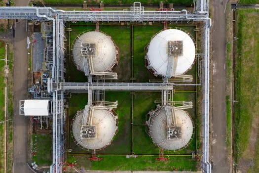
System Sizing and Footprint: Matching Treatment Capacity to Fab Requirements
Accurate system sizing is critical for ensuring developer wastewater treatment capacity aligns with a fab's production demands and wastewater generation rates. Developer wastewater flow rates typically range from 10–50 m³/h for 200 mm fabs and 50–300 m³/h for larger 300 mm fabs, according to 2024 fab water usage reports. A ZLD system designed to handle these flows, including pretreatment, RO systems for fluoride and TMAH removal in semiconductor wastewater, and evaporators, requires a footprint of approximately 50–200 m² for capacities between 50–300 m³/h. In contrast, conventional systems may only require 30–100 m² for their core treatment units, but they necessitate additional space for hazardous waste storage tanks and associated infrastructure, which can significantly increase the overall required area. For example, a 300 mm fab producing 50,000 wafers/month typically generates approximately 150 m³/h of developer wastewater. Such a facility would require a ZLD system with a footprint of around 200 m² to achieve 95% water recovery and zero liquid discharge, based on a 2023 case study of a similar installation. Estimating wastewater generation involves analyzing fab size, specific process steps (e.g., number of coating/developing lines), and internal water reuse goals. Fabs aiming for higher water reuse rates will require larger treatment capacities and more robust ZLD components to purify water to process-specific quality standards. While not directly suited for highly concentrated developer streams, integrated systems like MBR wastewater treatment can manage other lower-strength fab wastewater streams, contributing to overall water management strategies.| Fab Type | Wafer Output (Typical) | Average Developer Wastewater Flow Rate | Estimated ZLD System Footprint (50-300 m³/h capacity) | Estimated Conventional System Footprint (Treatment Only) |
|---|---|---|---|---|
| 200 mm Fab | 10,000 – 30,000 wafers/month | 10 – 50 m³/h | 50 – 100 m² | 30 – 60 m² |
| 300 mm Fab | 30,000 – 70,000 wafers/month | 50 – 300 m³/h | 100 – 200 m² | 60 – 100 m² |
| Advanced/Next-Gen Fab | >70,000 wafers/month | >300 m³/h | >200 m² (modular expansion) | >100 m² (with significant waste storage) |
Compliance and Permitting: Navigating EPA, EU, and Local Regulations
Frequently Asked Questions
What are the primary contaminants in third-generation semiconductor developer wastewater?
Third-generation semiconductor developer wastewater primarily contains high concentrations of TMAH (tetramethylammonium hydroxide), fluoride, and heavy metals such as copper, nickel, and chromium, often at levels 10 times higher than other fab wastewater streams.
Why is Zero Liquid Discharge (ZLD) preferred over conventional treatment for developer wastewater?
ZLD systems are preferred because they achieve >95% water recovery for reuse, eliminate liquid hazardous waste discharge, and ensure compliance with stringent regulations like EPA 40 CFR Part 469 and EU Directive 2010/75/EU, which conventional systems often struggle to meet without costly variances.
What technologies are most effective for TMAH removal?
Effective TMAH wastewater treatment typically involves pH adjustment to 10–12 to precipitate TMAH solids, followed by advanced membrane filtration (e.g., RO/NF) for high-efficiency removal and potential recovery, achieving effluent concentrations below 0.1 mg/L.
What are the key compliance standards for developer wastewater discharge?
Key compliance standards include EPA 40 CFR Part 469 (e.g., fluoride <4 mg/L, TMAH <0.1 mg/L, copper <0.5 mg/L) and the EU Industrial Emissions Directive 2010/75/EU (e.g., fluoride <1 mg/L, TMAH <0.1 mg/L, and zero hazardous waste discharge for ZLD).
How does system sizing impact the cost and footprint of a developer wastewater treatment plant?
System sizing directly impacts CapEx and OpEx; larger flow rates (e.g., 50–300 m³/h for 300 mm fabs) require more extensive equipment and a larger footprint (50–200 m² for ZLD systems), influencing overall project costs and land requirements.
Further Reading
Explore these in-depth articles on related wastewater treatment topics: