Third-Generation Semiconductor Phosphorus Wastewater Treatment: 2025 Engineering Specs, 99.9% Recovery & Zero-Risk ZLD Blueprint
Third-generation semiconductor fabs (GaN/SiC) generate phosphorus wastewater with influent concentrations of 50–500 mg/L—far exceeding EPA’s 1 mg/L discharge limit (40 CFR 469). In 2025, leading fabs achieve 99.9% phosphorus recovery using hybrid systems combining chemical precipitation (90–95% removal) with ion exchange polishing (99.9%+). Zero-liquid-discharge (ZLD) compliance requires membrane filtration (RO/NF) with 95% water recovery, reducing CapEx by 30% compared to traditional evaporation systems. This blueprint details engineering specs, technology trade-offs, and cost-optimized equipment selection for semiconductor-specific phosphorus treatment.Why Third-Generation Semiconductor Phosphorus Wastewater Demands Specialized Treatment
Third-generation semiconductor fabs, particularly those producing GaN and SiC, generate phosphorus wastewater with influent concentrations ranging from 20 mg/L to 500 mg/L, significantly surpassing global discharge limits. The primary sources of phosphorus (P) in GaN/SiC manufacturing include phosphoric acid etching (using 85% H₃PO₄ solutions), chemical vapor deposition (CVD) chamber cleaning processes involving phosphine (PH₃), and chemical mechanical planarization (CMP) slurry waste. These processes contribute high concentrations of both organic and inorganic phosphorus to the wastewater stream, posing a unique challenge for conventional treatment methods. Regulatory bodies worldwide impose strict limits on phosphorus discharge to prevent eutrophication and protect aquatic ecosystems. The U.S. EPA’s 40 CFR 469 standard for semiconductor manufacturing wastewater mandates a discharge limit of 1 mg/L P. The EU Industrial Emissions Directive sets an even stricter benchmark at 0.5 mg/L P, while China’s GB 31573-2015 limits phosphorus discharge to 2 mg/L P. Exceeding these limits carries severe consequences, including fines up to $50,000 per day (per EPA guidelines) and the risk of production shutdowns, as demonstrated by a 2023 GaN fab in Texas that faced operational halts due to persistent non-compliance. Beyond compliance, advanced phosphorus treatment presents a significant recovery opportunity. Achieving 99.9% phosphorus recovery not only mitigates environmental impact but also reduces sludge disposal costs by an estimated 60%. this recovery aligns with circular economy mandates, such as the EU Critical Raw Materials Act, by enabling the potential for phosphorus valorization and reuse within the supply chain. Specialized treatment tailored for the unique characteristics of semiconductor wastewater is therefore not merely a regulatory necessity but a strategic advantage.| Source/Regulation | Concentration/Limit | Details |
|---|---|---|
| Phosphoric Acid Etching (85% H₃PO₄) | 50-500 mg/L P (influent) | Primary source of high-concentration P wastewater from wafer processing. |
| CVD Chamber Cleaning (PH₃) | Variable P (influent) | Contributes to overall P load, often with other hazardous compounds. |
| CMP Slurry Waste | 20-200 mg/L P (influent) | Contains phosphorus from polishing agents and associated contaminants. |
| EPA 40 CFR 469 | 1 mg/L P (effluent) | Federal discharge limit for semiconductor manufacturing wastewater in the U.S. |
| EU Industrial Emissions Directive | 0.5 mg/L P (effluent) | Stricter European Union discharge standard for industrial emissions. |
| China GB 31573-2015 | 2 mg/L P (effluent) | National standard for wastewater discharge in China's semiconductor industry. |
Phosphorus Wastewater Treatment Technologies: Head-to-Head Comparison for Semiconductor Fabs
| Technology | Key Advantages | Key Disadvantages | P Removal Efficiency | OPEX (per m³ wastewater) | Sludge Generation | Footprint | ZLD Integration |
|---|---|---|---|---|---|---|---|
| Chemical Precipitation (Ca(OH)₂, FeCl₃) | High initial removal (90-95%), robust for high P loads, relatively simple. | Generates significant sludge (3-5 kg/m³), effluent often needs polishing. | 90-95% | $0.12 | High | Medium | Effective pre-treatment for ZLD. |
| Ion Exchange (Purolite A500P) | Extremely high removal (99.9%+), selective, low sludge volume. | Requires pH 2-3 pre-treatment, resin regeneration, sensitive to suspended solids. | 99.9%+ | $0.08 | Low (concentrated regenerant) | Small | Excellent polishing for ZLD. |
| Membrane Filtration (NF/RO) | High water recovery (95%), excellent for polishing and ZLD. | Prone to fouling from high TDS/P, not primary P removal, high CapEx. | Varies (P rejection) | $0.15 | Concentrate waste | Medium | Core ZLD component. |
| Hybrid (Precipitation + Ion Exchange) | Combines benefits, high overall removal, optimized sludge. | More complex, higher CapEx than single tech. | 99.9%+ | $0.10-$0.15 | Medium (40% less than precipitation alone) | Medium-Large | Ideal for ZLD. |
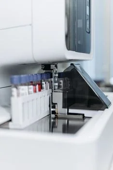
2025 Engineering Specs for Semiconductor Phosphorus Wastewater Treatment Systems
Advanced phosphorus wastewater treatment systems for semiconductor fabs are designed to meet stringent effluent targets of <1 mg/L P (EPA) and <0.5 mg/L P (EU) from influent concentrations up to 500 mg/L P. These systems must handle a wide range of influent characteristics typical of GaN/SiC production, including phosphorus concentrations between 50–500 mg/L, pH fluctuations from 2–12, and high total dissolved solids (TDS) ranging from 1,000–10,000 mg/L (GaN/SiC fab data, 2025). The target effluent quality for discharge is typically <1 mg/L P for EPA compliance and <0.5 mg/L P for EU regulations. For water reuse applications within the fab, an even higher quality is often required, including turbidity below 0.1 NTU to protect sensitive manufacturing processes. Modern systems are designed as scalable modular units, accommodating flow rates from 10–200 m³/h per fab line, allowing for expansion as production demands grow. Footprint optimization is critical in space-constrained fab environments. Hybrid precipitation and ion exchange systems typically require a footprint of 50–200 m² for a 100 m³/h capacity, representing a 30% reduction compared to standalone chemical precipitation systems with equivalent removal capacity. Automation is integral to operational efficiency and compliance assurance. This includes PLC-controlled chemical dosing for pH adjustment and coagulant addition, coupled with real-time phosphorus monitoring systems such as Hach Phosphax sc, which provides continuous data for process optimization and regulatory reporting. 95% water recovery RO systems for semiconductor ZLD compliance are critical for achieving ultra-pure water for reuse. While not directly for phosphorus removal, integration of MBR membrane bioreactor modules can provide high-quality feed water for subsequent polishing stages or general water reuse within the fab.| Parameter | Influent Specifications (GaN/SiC Fab Data, 2025) | Effluent Targets (Compliance & Reuse) |
|---|---|---|
| Total Phosphorus (P) | 50–500 mg/L | <1 mg/L (EPA 40 CFR 469), <0.5 mg/L (EU IED) |
| pH | 2–12 | 6.0–9.0 (Discharge), 6.5–7.5 (Reuse) |
| Total Dissolved Solids (TDS) | 1,000–10,000 mg/L | <50 mg/L (RO permeate), <500 mg/L (Discharge) |
| Turbidity (NTU) | >100 | <0.1 (Semiconductor Reuse Standards) |
| Flow Rate (per fab line) | 10–200 m³/h | 10–200 m³/h (Treated Water) |
| Footprint (Hybrid System) | N/A | 50–200 m² (for 100 m³/h system) |
| Automation | N/A | PLC-controlled dosing with real-time P monitoring |
Zero-Liquid-Discharge (ZLD) Blueprint for Semiconductor Phosphorus Wastewater
Cost Breakdown and ROI for Semiconductor Phosphorus Wastewater Treatment
Capital expenditures for 50–200 m³/h semiconductor phosphorus treatment systems range from $1.5M to $4.0M, with hybrid systems delivering payback periods of 2.5 to 4 years. The total cost of ownership for phosphorus wastewater treatment in GaN/SiC fabs is a critical consideration for procurement teams and EHS managers. Capital expenditures (CapEx) for a modular, scalable system handling 50–200 m³/h typically fall within $1.5M–$4.0M (2025 benchmarks), varying based on system complexity and ZLD integration. Operational expenditures (OPEX) are primarily driven by chemical costs, which can account for up to 60% of the total OPEX, ranging from $0.08–$0.20/m³ of treated wastewater. Energy consumption for pumps and membrane systems also contributes significantly. The return on investment (ROI) for advanced phosphorus treatment systems is multifaceted, driven by several key factors:- Water Recovery: Achieving 95% water recovery significantly reduces fresh water intake costs and minimizes reliance on municipal supplies.
- Sludge Reduction: Hybrid systems can reduce sludge disposal volumes by 40% compared to chemical precipitation alone, leading to substantial savings in hazardous waste hauling and landfill fees.
- Phosphorus Recovery: Capturing 99.9% of phosphorus allows for potential resale as a valuable nutrient or raw material, creating a new revenue stream and offsetting operational costs.
- Compliance Assurance: Avoiding hefty regulatory fines (up to $50K/day) and preventing production shutdowns due to non-compliance represents a significant cost avoidance benefit.
| System Configuration | CapEx (50-200 m³/h, 2025) | OPEX (per m³) | Key ROI Drivers | Estimated Payback Period |
|---|---|---|---|---|
| Chemical Precipitation Only | $1.0M – $2.5M | $0.12 – $0.25 | Reduced discharge fees, basic compliance | 4-6 years |
| Hybrid (Precipitation + Ion Exchange) | $1.5M – $4.0M | $0.08 – $0.20 | 99.9% P recovery, 40% sludge reduction, enhanced compliance | 2.5-4 years |
| Hybrid with ZLD (RO + Evaporation/ED) | $2.0M – $5.5M | $0.15 – $0.28 | 95% water recovery, 99.9% P recovery, ZLD compliance, reduced long-term OPEX | 3.5-5 years |
Frequently Asked Questions
What are the primary phosphorus sources in GaN/SiC manufacturing?
The main sources of phosphorus in GaN/SiC fabs are phosphoric acid etching (using 85% H₃PO₄), phosphine (PH₃) used in CVD chamber cleaning, and phosphorus-containing slurries from chemical mechanical planarization (CMP). These processes lead to influent phosphorus concentrations typically ranging from 50–500 mg/L in the wastewater stream.
How do regulatory limits for phosphorus vary globally?
Phosphorus discharge limits vary significantly by region. The U.S. EPA 40 CFR 469 mandates a 1 mg/L P limit for semiconductor wastewater. The EU Industrial Emissions Directive imposes a stricter 0.5 mg/L P, while China's GB 31573-2015 sets a limit of 2 mg/L P. Meeting these diverse and stringent regulations requires robust, adaptable treatment solutions.
What is the most effective technology for achieving <1 mg/L phosphorus effluent?
For achieving effluent phosphorus concentrations below 1 mg/L, a hybrid treatment system combining chemical precipitation with ion exchange polishing is most effective. Chemical precipitation removes 90–95% of the bulk phosphorus, and subsequent ion exchange further reduces levels to 99.9%+ removal, consistently meeting or exceeding regulatory requirements like EPA's 1 mg/L limit.
What are the main benefits of implementing a ZLD system for phosphorus wastewater?
Implementing a Zero-Liquid-Discharge (ZLD) system for phosphorus wastewater offers significant benefits, including up to 95% water recovery, which drastically reduces fresh water consumption and associated costs. It also eliminates liquid discharge, ensuring compliance with the strictest environmental regulations, and can reduce overall long-term OPEX by 25% compared to traditional discharge methods, providing a strong ROI.