Third-generation semiconductor electroplating wastewater contains Ga, SiC, TMAH, and heavy metals (Cr, Ni, Cu) at ppb-ppm levels, requiring hybrid treatment systems to achieve 99.9% recovery and zero liquid discharge (ZLD). In 2025, fabs prioritize selective ion exchange for Ga/SiC recovery (95-99% efficiency) and membrane filtration (RO/NF) for TMAH removal, with CAPEX ranging from $2M–$10M for ZLD-compliant systems. Regulatory drivers include EPA’s 2024 semiconductor effluent guidelines and China’s GB 31573-2023, mandating <0.1 mg/L for total heavy metals.
Why Third-Generation Semiconductor Wastewater Is a Unique Treatment Challenge
Gallium Nitride (GaN) and Silicon Carbide (SiC) fabrication processes generate effluent streams that are significantly more complex than traditional silicon-based semiconductor or general electroplating wastewater. The primary challenge lies in the coexistence of high-value rare metals (Ga), abrasive particulates (SiC), and highly toxic organic developers like Tetramethylammonium hydroxide (TMAH), often suspended in a matrix of high-purity mineral acids. Unlike conventional industrial wastewater, these streams exhibit extreme pH fluctuations (pH 2–12) and contain "qualitative contaminants"—pollutants that are hazardous even at parts-per-billion (ppb) levels (Zhongsheng field data, 2025).
Conventional chemical precipitation often fails in these environments because high-purity acids used in cleaning steps (like Piranha or SPM) can corrode standard carbon steel or low-grade stainless steel treatment infrastructure. TMAH acts as a potent surfactant and biological inhibitor, causing massive foaming in aerobic digesters and rendering biological treatment ineffective without significant dilution or advanced oxidation. For GaN/SiC fabs, the focus shifts from simple "removal" to "selective recovery," as the market value of recovered Gallium and the high disposal costs of SiC-laden sludge ($1,200–$2,500/ton) dictate the economic viability of the treatment plant.
Regulatory pressure has intensified with the EPA’s 2024 semiconductor effluent guidelines, which now target total heavy metals at thresholds below 0.1 mg/L. Simultaneously, China’s GB 31573-2023 standard mandates TMAH concentrations below 1 mg/L for direct discharge, a limit that traditional municipal treatment plants cannot meet. These standards necessitate a transition toward hybrid ZLD systems that integrate selective ion exchange and high-pressure membrane separation.
| Parameter | Conventional Electroplating | 3rd Gen Semi (GaN/SiC) | Treatment Requirement |
|---|---|---|---|
| Primary Metals | Cu, Ni, Cr, Zn (10-100 mg/L) | Ga, SiC, Cr, Ni, Cu (ppb-50 mg/L) | Selective Recovery >95% |
| Organic Load | Low (BOD/COD <200 mg/L) | TMAH (50-500 mg/L) | Advanced Oxidation/RO |
| Abrasives | Minimal | SiC Nanoparticles (10-100 mg/L) | Ultrafiltration/DAF |
| Regulatory Target | <1.0 mg/L Total Metals | <0.1 mg/L Total Metals (EPA 2024) | ZLD / Hybrid Membrane |
Electroplating Wastewater Composition: A 2025 Fab Data Breakdown
Designing a resilient pretreatment system requires precise characterization of the influent, which varies based on whether the fab is running batch-type cleaning or continuous electroplating lines. In 2025, GaN-on-Si and SiC-on-SiC processes dominate the power electronics sector, each contributing unique chemical signatures to the wastewater stream. GaN lines typically show higher concentrations of Gallium (5–50 mg/L) following the etching and plating phases, while SiC lines produce higher Total Suspended Solids (TSS) due to the mechanical polishing and dicing of the extremely hard SiC substrate.
TMAH remains the most problematic organic component. Used extensively as a developer and etchant, TMAH is highly water-soluble and carries an LC50 of less than 10 mg/L for Daphnia magna, making it a critical target for EHS managers. Variability in tool-specific chemistries—such as the transition from APM (Ammonia-Peroxide Mixture) to proprietary solvent-based cleaners—can lead to sudden spikes in Nitrogen and COD, requiring PLC-controlled chemical dosing for precise pH adjustment and coagulant injection to prevent system upsets.
| Contaminant | GaN Electroplating Influent | SiC Electroplating Influent | 2025 Discharge Limit |
|---|---|---|---|
| Gallium (Ga) | 5 – 50 mg/L | <1 mg/L | <0.05 mg/L (Internal Reclaim) |
| Silicon Carbide (SiC) | <5 mg/L | 10 – 100 mg/L | <1 mg/L (TSS) |
| TMAH | 100 – 500 mg/L | 50 – 200 mg/L | <1 mg/L (GB 31573-2023) |
| Heavy Metals (Cr, Ni, Cu) | 0.5 – 10 mg/L | 0.1 – 5 mg/L | <0.1 mg/L (EPA 2024) |
| pH | 2.0 – 11.5 | 3.0 – 10.5 | 6.0 – 9.0 |
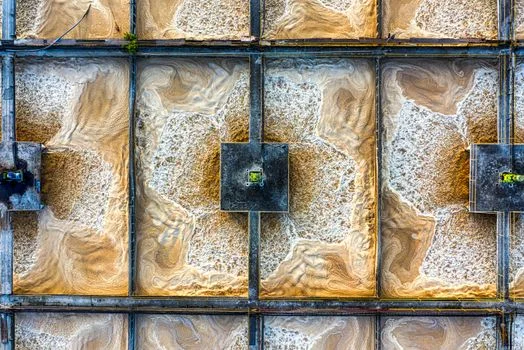
Toxicity risks are not limited to the liquid effluent. The sludge generated from GaN/SiC processes is often classified as hazardous waste due to the presence of heavy metal co-precipitants. In 2025, the cost of hauling and disposing of this sludge has risen to $2,500 per ton in high-regulation regions like the EU and Taiwan. This economic burden is the primary driver for fabs to adopt ZLD blueprints that minimize sludge volume while maximizing the purity of recovered metal salts.
Hybrid Treatment Technologies for 99.9% Heavy Metal Recovery
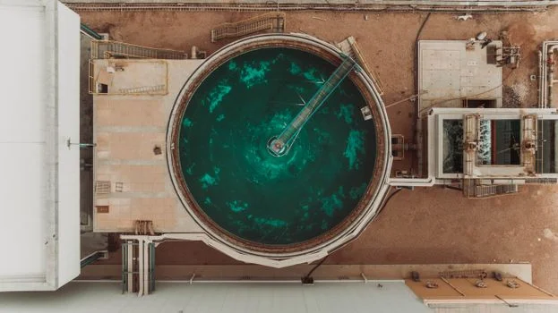
Achieving 99.9% recovery of heavy metals in a semiconductor environment requires a multi-stage hybrid approach. No single technology can cost-effectively handle the high acidity, high organic load, and trace metal concentrations simultaneously. The 2025 standard process flow begins with selective ion exchange (IX), followed by membrane concentration, and terminates in a ZLD unit.
Selective Ion Exchange for Ga/SiC Recovery: For Gallium recovery, chelation resins with aminophosphonic or iminodiacetic functional groups are utilized. These resins exhibit high selectivity for Ga³⁺ even in the presence of competing ions like Ca²⁺ or Mg²⁺. Engineers typically target a recovery rate of 95–99%, with regeneration costs maintained between $0.20–$0.50/m³ of treated water. For SiC, the focus is on solids capture using compact lamella clarifiers for sludge volume reduction prior to ion exchange to prevent resin fouling.
RO/NF for TMAH Removal: Tetramethylammonium ions (TMA+) are effectively rejected by thin-film composite polyamide membranes. Ultra-pure RO systems for TMAH removal and ZLD concentration are designed to operate at flux rates of 15–30 LMH. To prevent organic fouling caused by TMAH and photoresist residues, antiscalant dosing at 2–5 mg/L is mandatory. Nanofiltration (NF) is often used as a precursor to RO to separate divalent heavy metals from monovalent salts, simplifying the downstream crystallization process.
Chemical Precipitation for Heavy Metals: While IX handles the high-value recovery, bulk heavy metal removal (Cr, Ni, Cu) relies on staged pH adjustment. Hexavalent Chromium must first be reduced to Trivalent Chromium at pH 2–3 using sodium bisulfite before being precipitated as Cr(OH)₃ at pH 8–9. Nickel and Copper require higher pH levels (10–11) for optimal precipitation. To enhance settling, coagulants like FeCl₃ are dosed at 50–200 mg/L, followed by polymer flocculants.
| Technology | Target Contaminant | Removal/Recovery Efficiency | Operational Cost (OPEX) |
|---|---|---|---|
| Selective Ion Exchange | Ga, Ni, Cu | 98% - 99.9% | Medium ($0.35/m³) |
| High-Pressure RO | TMAH, TDS | >99% | High ($0.80/m³) |
| Advanced Oxidation (Fenton) | TMAH (Organic) | >90% (as COD) | Medium ($0.50/m³) |
| Lamella Clarification | SiC, Metal Hydroxides | >95% (TSS) | Low ($0.15/m³) |
The integrated process flow typically follows this sequence: 1. Influent Equalization -> 2. High-Efficiency Sedimentation (SiC removal) -> 3. Selective IX (Ga recovery) -> 4. Advanced Oxidation (TMAH breakdown) -> 5. RO/NF (Concentration) -> 6. ZLD Evaporation/Crystallization. This sequence ensures that the most valuable and most fouling-prone components are removed before reaching the expensive membrane and thermal stages.
Zero Liquid Discharge (ZLD) for Semiconductor Fabs: Engineering Specs and Compliance
Zero Liquid Discharge is no longer just a sustainability goal; it is a risk management strategy for fabs operating in water-stressed regions or under stringent discharge permits. A ZLD system for third-generation semiconductors must handle the high osmotic pressure of concentrated electroplating salts and the thermal stability of residual organics. The engineering blueprint involves three distinct phases: pretreatment, concentration, and crystallization.
Pretreatment for ZLD often utilizes a high-efficiency DAF for pretreatment of suspended solids and FOG that might have bypassed initial filtration. Once the stream is clarified, it enters the concentration phase. While thermal evaporators were once the only option, 2025 designs favor membrane-based ZLD (such as Disc Tube RO or Vibratory Shear Enhanced Processing) for the initial concentration step. This reduces energy consumption from 15 kWh/m³ (thermal) to approximately 4 kWh/m³ (membrane). The final step involves Mechanical Vapor Recompression (MVR) or spray dryers to produce a solid salt cake for disposal or potential byproduct reuse.
Compliance with the EPA 2024 guidelines is built into the ZLD design. By eliminating the liquid discharge point entirely, the fab avoids the need for continuous effluent monitoring for <0.1 mg/L heavy metals at the outfall. However, the internal distillate must still meet high-purity standards if it is to be reused. Typical ZLD distillate quality targets <1 mg/L TMAH and <10 mg/L TDS. For more complex streams involving multiple dopants, engineers should refer to the arsenic-specific ZLD blueprint for semiconductor fabs to ensure co-precipitation risks are managed.
A recent case study of a 500 m³/day GaN fab in Taiwan illustrates the ROI of this approach. By installing a hybrid ZLD system, the facility reduced its hazardous waste hauling volume by 92% and recovered enough Gallium to offset 15% of its raw material costs. With a total CAPEX of $8M, the system achieved a payback period of 4.2 years, primarily through the elimination of regulatory fine risks and the reduction in fresh water procurement costs.
Cost Breakdown: CAPEX, OPEX, and ROI for Semiconductor Wastewater Treatment
Procurement teams must balance the high initial investment of ZLD with the long-term operational risks of non-compliance. In 2025, the cost of wastewater treatment is categorized into three pathways: Conventional (Compliance-only), Hybrid (Recovery-focused), and ZLD (Zero-risk). While conventional systems have the lowest CAPEX, they carry the highest risk of regulatory fines and provide no value through metal recovery.
For a 1,000 m³/day fab, a hybrid system focusing on copper recovery strategies for semiconductor electroplating and gallium ion exchange typically requires a CAPEX of $4M–$6M. However, the OPEX is partially offset by the "circular economy" value of the recovered metals. In contrast, a full ZLD system for the same capacity may cost $12M–$15M but provides a "future-proof" solution against evolving EPA and local standards.
| System Scale | Treatment Pathway | Estimated CAPEX | Annual OPEX (incl. Sludge) | Compliance Level |
|---|---|---|---|---|
| 200 m³/day | Conventional | $0.8M - $1.2M | $250,000 | Moderate Risk |
| 200 m³/day | Hybrid (IX + RO) | $2.0M - $3.5M | $180,000 | High |
| 1,000 m³/day | Hybrid (IX + RO) | $5.0M - $8.0M | $650,000 | High |
| 1,000 m³/day | Full ZLD (MVR) | $12M - $18M | $1,200,000 | Zero Risk |
The ROI calculation for ZLD adoption should include "hidden" savings. For instance, regulatory fines for exceeding heavy metal limits can range from $50,000 to $250,000 per violation, and persistent non-compliance can lead to permit delays of 6–12 months for fab expansions. When factoring in the $1.5M/year savings in disposal costs for a 1,000 m³/day facility, the transition to ZLD often presents a more favorable net present value (NPV) over a 10-year horizon than conventional treatment.
Frequently Asked Questions
Q: What’s the most cost-effective treatment for GaN electroplating wastewater?
A: Selective ion exchange for Ga recovery (95–99% efficiency) combined with RO for TMAH removal is the most cost-effective approach. This hybrid method reduces the volume of waste entering the ZLD stage, lowering total CAPEX by 30–40% compared to direct evaporation of the entire waste stream.
Q: How do I comply with EPA’s 2024 semiconductor effluent guidelines?
A: Compliance requires real-time monitoring and automated dosing. Implementing ICP-MS monitoring for influent streams and automated pH adjustment (±0.1 units) is critical to ensure heavy metals stay below the <0.1 mg/L threshold. For organic compliance, refer to TMAH-specific treatment technologies for semiconductor fabs.
Q: What’s the biggest mistake fabs make with wastewater treatment?
A: Underestimating the impact of TMAH on biological and membrane systems. TMAH causes severe foaming and is toxic to the microbes in traditional activated sludge. Fabs should always pretreat TMAH-rich streams with chemical oxidation (e.g., Fenton’s reagent) or high-rejection RO before any biological or thermal process.
Q: Can I reuse treated semiconductor wastewater for process water?
A: Yes, but it requires tertiary polishing. Treated effluent from a ZLD or RO system must pass through Electrodeionization (EDI) to achieve conductivity levels <10 µS/cm for reuse in cooling towers, scrubbers, or as makeup water for UPW (Ultra-Pure Water) systems. Most modern fabs successfully reuse 30–50% of their treated wastewater.