Achieving stringent compliance for nickel in PCB wastewater necessitates 99.9% nickel recovery, targeting effluent limits such as GB 39731-2020's <0.5 mg/L and EPA's <2.38 mg/L. Modern treatment systems typically integrate chemical precipitation (optimizing pH 9–10 with 100–200 mg/L NaOH dosing) with advanced polishing via ion exchange (achieving 95–99% nickel removal) or membrane filtration (where VSEP RO can reach <0.1 mg/L effluent). Implementing zero liquid discharge (ZLD) systems, exemplified by closed-loop designs achieving 45 gpm, eliminates substantial hauling costs ($0.50–$2.00/gallon) and enables 90%+ water reuse for critical plating rinse lines.
Why Nickel in PCB Wastewater Is a Compliance Nightmare
Nickel is a persistent heavy metal contaminant in PCB electroplating wastewater, posing significant compliance challenges for electronics manufacturers. Nickel is extensively used in processes like electroless nickel/gold (ENIG), nickel-palladium-gold (ENEPIG), and certain etching steps, generating rinse waters with typical nickel concentrations ranging from 5–50 mg/L, as outlined in EPA 2023 PCB effluent guidelines. This makes effective printed circuit board nickel wastewater treatment a critical operational concern.
Strict regulatory frameworks govern nickel discharge globally; for instance, China's GB 39731-2020 sets a stringent nickel discharge limit of <0.5 mg/L, while EPA 40 CFR 469 requires effluent to be below <2.38 mg/L. Non-compliance with these limits can trigger severe penalties, including fines ranging from $10,000 to $50,000 per violation, and potentially lead to costly production halts. Traditional wastewater treatment methods, such as basic hydroxide precipitation, frequently fail to achieve these stringent limits, particularly when nickel is complexed with organic agents like EDTA or citric acid commonly found in PCB manufacturing wastewater. A real-world example demonstrates this challenge: a Northeastern PCB facility previously struggled with consistent nickel violations but significantly reduced them by 98% after transitioning from batch precipitation to a continuous ion exchange and reverse osmosis (RO) system (Aries case study). This highlights the necessity of advanced nickel removal efficiency for sustained compliance.
Nickel Removal Mechanisms: Chemical Precipitation, Ion Exchange, and Membrane Filtration
printed circuit board nickel wastewater treatment - Nickel Removal Mechanisms: Chemical Precipitation, Ion Exchange, and Membrane Filtration
Effective nickel removal from PCB wastewater relies on a combination of proven and emerging technologies, each with distinct mechanisms and performance characteristics. Understanding these allows engineers to select the most appropriate solution for their specific influent conditions and compliance targets.
Chemical Precipitation
Chemical precipitation is a foundational method for nickel removal, where nickel hydroxide forms at an alkaline pH range of 9–10, typically achieved by dosing with NaOH or Ca(OH)₂. This process can achieve 90–95% removal efficiency for free nickel ions. However, its effectiveness drops significantly to less than 70% when nickel is complexed with organic ligands like EDTA, which are prevalent in PCB manufacturing wastewater, necessitating further treatment.
Ion Exchange
Ion exchange for heavy metals utilizes chelating resins, often containing iminodiacetic acid functional groups, which selectively bind nickel ions from the wastewater stream. These systems demonstrate high nickel removal efficiency, typically achieving 95–99% at optimal flow rates of 10–20 bed volumes per hour (BV/h). Regeneration of the resin column is required every 2–4 hours for continuous operation, usually involving a 5–10% HCl or H₂SO₄ solution, completing a cycle in approximately 2–4 hours.
Membrane Filtration
Membrane filtration, particularly reverse osmosis (RO) systems, provides superior nickel removal, with advanced vibrating membrane systems like VSEP RO achieving effluent nickel concentrations below <0.1 mg/L. This level of reverse osmosis for nickel recovery typically requires robust pre-treatment, such as microfiltration at 0.1–0.5 µm, to prevent membrane fouling from particulates and colloids. Typical flux rates for PCB wastewater in RO systems range from 15–30 LMH (liters per square meter per hour).
Electrocoagulation
Electrocoagulation is an emerging technology for nickel removal, offering 85–95% efficiency by introducing metal ions (e.g., iron, aluminum) into the wastewater via sacrificial electrodes. While promising, its widespread scalability can be limited by relatively high energy consumption, typically 0.5–1.5 kWh/m³.
Technology
Mechanism
Nickel Removal Efficiency
Key Parameters
Limitations
Chemical Precipitation
Forms insoluble nickel hydroxide
90–95% (free Ni), <70% (complexed Ni)
pH 9–10 (NaOH, Ca(OH)₂ dosing)
Ineffective for complexed Ni, generates sludge
Ion Exchange
Selective binding by chelating resins
95–99%
Flow rate 10–20 BV/h, Regeneration with acid
Resin fouling, regeneration waste, sensitive to organics
Membrane Filtration (RO)
Physical separation via semi-permeable membrane
>99% (<0.1 mg/L effluent)
Pre-treatment (MF 0.1–0.5 µm), Flux 15–30 LMH
Membrane fouling, high pressure, concentrate disposal
Electrocoagulation
Electrolytic generation of coagulants
85–95%
Energy use 0.5–1.5 kWh/m³
High energy consumption, electrode passivation
Engineering Specs for PCB Nickel Wastewater Treatment Systems
Precise engineering parameters are critical for designing and operating robust PCB heavy metal wastewater treatment systems to ensure consistent nickel removal efficiency and compliance. Influent characteristics from PCB manufacturing vary significantly, typically containing nickel at 5–50 mg/L, copper at 10–100 mg/L, a pH range of 2–12, TSS (Total Suspended Solids) from 50–500 mg/L, and COD (Chemical Oxygen Demand) from 200–2,000 mg/L (Zhongsheng field data, 2025).
For effective chemical precipitation, automated pH and coagulant dosing for nickel precipitation is paramount. Sodium hydroxide (NaOH) dosing of 100–200 mg/L is common to achieve the optimal pH of 9–10 for nickel hydroxide precipitation. Coagulants such as ferric chloride (FeCl₃) at 30–50 mg/L are often added to aid floc formation and improve settling. Maintaining pH control within ±0.2 units is critical for stable precipitation and consistent nickel hydroxide precipitation.
In ion exchange systems, the resin bed depth is typically 1–1.5 m, designed to provide a contact time of 5–10 minutes for efficient nickel adsorption. Regeneration frequencies range from every 2–4 hours at a flow rate of 10–20 BV/h, depending on the influent nickel load and resin capacity.
Membrane systems for nickel removal, particularly RO, operate at pressures of 15–30 bar to achieve recovery rates of 70–85%. Membrane cleaning is typically performed every 1–2 weeks, involving alternating alkaline and acid washes to remove foulants and maintain flux. Sludge handling is a significant consideration; nickel hydroxide sludge, typically 2–5% solids, requires dewatering using a plate/frame filter press for nickel sludge dewatering operating at 5–10 bar to achieve 20–30% solids content. This dewatered sludge must then meet landfill TCLP (Toxicity Characteristic Leaching Procedure) limits, typically <5 mg/L leachable nickel.
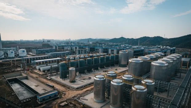
Zero Liquid Discharge (ZLD) for PCB Nickel Wastewater: Costs, Recovery Rates, and ROI
printed circuit board nickel wastewater treatment - Zero Liquid Discharge (ZLD) for PCB Nickel Wastewater: Costs, Recovery Rates, and ROI
Implementing zero liquid discharge for electronics manufacturing offers significant environmental and economic benefits by eliminating wastewater discharge and maximizing water reuse. A typical ZLD system for PCB nickel wastewater integrates several stages: initial chemical pre-treatment to remove bulk contaminants, followed by microfiltration (0.1–0.5 µm) for suspended solids and colloidal removal. The pre-treated water then undergoes RO systems for nickel removal and water reuse, operating at 15–30 bar, to concentrate the dissolved solids. The resulting high-purity permeate is reused, while the concentrated brine is further treated via evaporation and crystallization to achieve complete ZLD.
The capital expenditure (CAPEX) for ZLD systems treating 10–100 m³/h (45–450 gpm) of PCB wastewater typically ranges from $500,000 to $2,000,000, based on 2025 data scaled from recent industry case studies. Operational expenditure (OPEX) for these systems is estimated at $0.10–$0.30/m³. This breaks down into energy costs of $0.05–$0.15/m³, chemical costs of $0.03–$0.10/m³, and membrane replacement costs of $0.02–$0.05/m³. These wastewater treatment CAPEX OPEX figures highlight the long-term economic viability.
Significant savings are realized through ZLD implementation. Eliminating wastewater hauling costs, which range from $0.50–$2.00/gallon ($0.13–$0.53/liter), provides immediate financial relief. the high water reuse rate of 90–95% substantially reduces municipal water consumption costs by 60–80%. Based on a typical water cost of $1.50/m³ and a hauling cost of $0.80/gallon, the return on investment (ROI) for ZLD systems treating 50–100 m³/day can be achieved within 2–4 years.
Cost/Savings Category
Range/Value
Notes
CAPEX (10–100 m³/h system)
$500,000 – $2,000,000
Includes pre-treatment, MF, RO, evaporation/crystallization
OPEX (per m³ treated)
$0.10 – $0.30
Energy, chemicals, membrane replacement, labor
Energy Cost (per m³)
$0.05 – $0.15
Primary component of OPEX
Chemical Cost (per m³)
$0.03 – $0.10
Coagulants, pH adjusters, antiscalants
Membrane Replacement (per m³)
$0.02 – $0.05
Depreciation and replacement of RO membranes
Hauling Cost Elimination (per gallon)
$0.50 – $2.00
Direct savings from not discharging/hauling wastewater
Water Reuse Rate
90% – 95%
Reduction in municipal water intake
Municipal Water Cost Reduction
60% – 80%
Based on reduced fresh water consumption
ROI (for 50–100 m³/day system)
2 – 4 years
Calculated based on average water and hauling costs
Compliance Mapping: Global Nickel Discharge Limits and Treatment Requirements
Navigating global nickel discharge limits is essential for PCB manufacturers to ensure regulatory adherence and avoid penalties, as standards vary significantly by region. China's national standard, GB 39731-2020 compliance guide for PCB manufacturers, sets a stringent daily maximum nickel limit of <0.5 mg/L and a monthly average of <0.2 mg/L for industrial wastewater discharge.
In the United States, the EPA 40 CFR 469 (Electronics Manufacturing) mandates a monthly average nickel discharge limit of <2.38 mg/L. However, local Publicly Owned Treatment Works (POTWs) often impose significantly stricter limits, with some regions, such as parts of California, requiring effluent nickel concentrations below <0.1 mg/L.
The European Union's Industrial Emissions Directive (IED) 2010/75/EU establishes Best Available Technology Associated Emission Levels (BAT-AELs) for direct discharges, which typically require nickel concentrations to be below <0.1 mg/L. India's Central Pollution Control Board (CPCB) guidelines, updated in 2022, set a nickel limit of <1.0 mg/L for PCB manufacturing facilities.
To account for influent variability and ensure consistent compliance, treatment systems should be designed with an effluent target that is 2–3 times below the regulatory limit. For example, to meet the EU's <0.1 mg/L limit, a system should be engineered to consistently achieve <0.03–0.05 mg/L nickel in the effluent.
Region/Standard
Nickel Discharge Limit
Notes
China (GB 39731-2020)
<0.5 mg/L (Daily Max), <0.2 mg/L (Monthly Avg)
Strict national standard for electronics industry
USA (EPA 40 CFR 469)
<2.38 mg/L (Monthly Avg)
Federal guideline; local POTWs may impose stricter limits
USA (California POTW example)
<0.1 mg/L
Example of a stricter local limit
EU (IED 2010/75/EU - BAT-AEL)
<0.1 mg/L
Best Available Technology Associated Emission Level for direct discharge
India (CPCB 2022)
<1.0 mg/L
National guidelines for PCB manufacturers
How to Select the Right Nickel Wastewater Treatment System for Your PCB Plant
printed circuit board nickel wastewater treatment - How to Select the Right Nickel Wastewater Treatment System for Your PCB Plant
Selecting the optimal nickel wastewater treatment system requires a structured decision-making process to match technology capabilities with specific plant needs and regulatory demands. The first critical step is to comprehensively characterize the wastewater influent, including nickel speciation (e.g., free vs. complexed nickel), total flow rate, and the presence of co-contaminants like copper, organics, and chelating agents. Utilizing advanced analytical techniques such as ion chromatography is essential for accurately quantifying complexed nickel (e.g., EDTA-Ni), which significantly impacts treatment strategy.
Step 2 involves clearly defining compliance targets, encompassing local discharge limits and any zero liquid discharge (ZLD) goals. For facilities facing stringent limits (e.g., <0.1 mg/L), prioritizing technologies capable of 99%+ nickel removal, such as integrated RO and ion exchange systems, is imperative. The third step focuses on evaluating the system's physical footprint and automation requirements. For instance, compact MBR systems for PCB wastewater treatment can save space but may require more skilled operators, whereas chemical precipitation systems are generally lower-maintenance but offer less efficient nickel removal.
Step 4 requires a thorough modeling of costs, including both CAPEX (capital expenditure) and OPEX (operational expenditure), and a detailed ROI analysis. Leveraging the cost table from the ZLD section can help compare the long-term financial implications of wastewater hauling versus investing in an on-site treatment system. Finally, Step 5 is to pilot test the top 2–3 viable options on-site. Reputable vendors like Zhongsheng Environmental offer skid-mounted pilot units (typically 1–5 m³/h capacity) for real-world validation of performance, allowing for optimization before full-scale deployment.
What is the most cost-effective nickel removal technology for PCB wastewater?
Ion exchange is generally cost-effective for smaller flow rates (<20 m³/h) with moderate nickel levels (5–20 mg/L), offering good nickel removal efficiency. Reverse osmosis (RO) becomes more economically viable for larger flows (>50 m³/h) or when zero liquid discharge (ZLD) is a goal due to its high water recovery and superior effluent quality. Chemical precipitation is the cheapest upfront investment but typically requires secondary polishing to meet stringent compliance limits, adding to overall cost.
How do I reduce nickel sludge disposal costs?
Reducing nickel sludge disposal costs involves several strategies. First, dewater sludge to 20–30% solids content using a plate/frame filter press for nickel sludge dewatering operating at 5–10 bar pressure. This significantly reduces volume and associated hauling costs. Second, stabilize the dewatered sludge with lime to achieve a pH of 12, ensuring it passes TCLP (Toxicity Characteristic Leaching Procedure) tests for non-hazardous landfill disposal. Some advanced facilities explore recovering nickel from sludge via acid leaching, which can achieve 80–90% recovery, converting a waste stream into a valuable resource.
Can I reuse treated nickel wastewater in PCB manufacturing?
Yes, treated nickel wastewater can be reused in PCB manufacturing, particularly if processed through advanced systems. RO permeate, which can achieve <0.1 mg/L nickel, is suitable for reuse in non-critical rinse lines, significantly reducing fresh water consumption. For ultra-pure water applications, such as DI water makeup, the RO permeate may require further polishing, often through a mixed-bed ion exchange system, to meet stringent purity specifications. This enables substantial water savings and contributes to zero liquid discharge for electronics manufacturing goals.
What are the common failure points in nickel wastewater treatment systems?
Common failure points include fouling of RO systems for nickel removal and water reuse membranes due to high organic loads, silica scaling, or particulate buildup, leading to reduced flux and increased cleaning frequency. In ion exchange systems, resin poisoning from oils, surfactants, or complexing organics can reduce resin capacity and nickel removal efficiency. pH control failures in chemical precipitation are also critical, as deviations from the optimal pH 9–10 range can result in incomplete nickel removal and non-compliant effluent. Regular maintenance and proper pre-treatment are crucial to mitigate these issues.
How do I comply with GB 39731-2020 for nickel in China?
To comply with GB 39731-2020 nickel limits in China, which are <0.5 mg/L daily max and <0.2 mg/L monthly avg, it is recommended to design your treatment system for an effluent target of <0.2 mg/L nickel, providing a safety margin. This typically requires a two-stage system, combining chemical precipitation (optimizing at pH 9.5) followed by a polishing step such as ion exchange or reverse osmosis. Implementing online nickel monitors (e.g., using ICP-OES technology) for real-time compliance tracking and automatic system adjustments is also a best practice.
Zhongsheng Engineering Team
Our team of wastewater treatment engineers has over 15 years of experience designing and manufacturing DAF systems, MBR bioreactors, and packaged treatment plants for clients in 30+ countries worldwide.