Semiconductor effluent standards are governed by region-specific regulations, with the US EPA’s 40 CFR Part 469 setting fluoride limits below 15 ppm for direct dischargers, while SEMI F116 (2021) provides water reuse guidelines for fabs. Global standards vary: China’s GB 39731-2020 mandates total phosphorus <0.5 mg/L, and Taiwan’s regulations require TSS <30 ppm. Treatment systems must achieve 95%+ fluoride removal and 99% TSS reduction to meet these limits, with dissolved air flotation (DAF) and membrane bioreactors (MBR) as proven solutions for semiconductor wastewater.
Why Semiconductor Effluent Standards Are Tightening in 2025
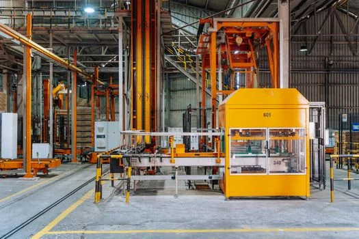
Semiconductor fabs consume 2–4 million gallons of water per day per SEMI 2023 data, with 30–50% discharged as wastewater containing fluoride, heavy metals, and total suspended solids (TSS). The environmental pressure on the industry has intensified as the global semiconductor market expands, leading to a direct correlation between production volume and localized environmental impact. Fluoride toxicity in aquatic ecosystems, with an LC50 for fish ranging between 50–100 ppm, is the primary driver for stricter discharge limits. Consequently, the US EPA is currently evaluating a draft rule for 2026 that proposes lowering the fluoride limit to 10 ppm for specific subcategories.
Water scarcity in critical manufacturing hubs like Taiwan and Arizona has transformed wastewater management from a compliance obligation into a business continuity necessity. Local ordinances now frequently require 85%+ water reuse rates for new fabs, a standard exemplified by TSMC’s Arizona facility. the 2023 EPA study on the Electrical and Electronic Components (E&EC) category expansion has clarified that semiconductor fabs are explicitly covered under 40 CFR Part 469, effectively removing the ambiguity that previously allowed some facilities to operate under less stringent Metal Finishing standards (40 CFR Part 433).
The tightening of these standards also reflects the increasing complexity of semiconductor chemistry. As nodes shrink below 5nm, the use of specialized chemicals in Chemical Mechanical Planarization (CMP) and photolithography increases the concentration of refractory organics and nano-sized particles in the effluent. Meeting the semiconductor effluent standard in 2025 requires a shift from passive treatment to active, high-precision engineering solutions that address both dissolved and suspended pollutants with zero margin for error.
Global Semiconductor Effluent Standards Compared: US, EU, China, Taiwan, and Korea
Discharge limits for fluoride in the semiconductor industry are converging globally toward a 10–15 ppm threshold to mitigate bioaccumulation in aquatic ecosystems. However, significant variations exist regarding nutrient removal (nitrogen and phosphorus) and heavy metal thresholds, which dictate the complexity of the required zero liquid discharge (ZLD) systems for semiconductor fabs.
| Pollutant Parameter | US EPA (40 CFR 469) | China (GB 39731-2020) | Taiwan (EPA 2024) | EU IED (BAT-AEL) | South Korea (WQA) |
|---|---|---|---|---|---|
| Fluoride (F-) | < 15 mg/L (Daily Max) | < 10 mg/L | < 15 mg/L | < 15 mg/L | < 15 mg/L |
| TSS | Permit-specific (< 30 mg/L) | < 20 mg/L | < 30 mg/L | < 20 mg/L | < 30 mg/L |
| COD | N/A | < 50 mg/L (Varies) | < 100 mg/L | < 100 mg/L | < 40 mg/L |
| Total Phosphorus | N/A | < 0.5 mg/L | N/A | < 1.0 mg/L | < 0.5 mg/L |
| Copper (Cu) | N/A | < 0.3 mg/L | < 1.0 mg/L | < 0.5 mg/L | < 0.1 mg/L |
| Ammonia-Nitrogen | N/A | < 8 mg/L (Shanghai) | < 20 mg/L | < 15 mg/L | < 10 mg/L |
In the United States, 40 CFR Part 469 mandates a pH range of 6.5–9.0, but does not explicitly set a federal TSS limit, leaving that to state-level NPDES permits which typically cap TSS at 30 ppm. Conversely, China’s GB 39731-2020 standards for semiconductor wastewater are among the strictest in the world for nutrient control, requiring advanced biological treatment to meet phosphorus and nitrogen limits. The EU’s Industrial Emissions Directive (IED) focuses heavily on Best Available Techniques (BAT), with stringent limits on nickel (<0.1 mg/L) and copper, reflecting the Water Framework Directive's goal of achieving "good status" for all water bodies.
Pollutant-Specific Treatment Technologies: Engineering Specs for Fluoride, TSS, and Heavy Metals
Effective fluoride removal in semiconductor wastewater requires reducing influent concentrations from 500 ppm to below 15 ppm using multi-stage chemical precipitation and flotation. For high-concentration fluoride streams, calcium chloride (CaCl₂) or lime dosing is utilized to form calcium fluoride (CaF₂) precipitates. Engineering specs for DAF systems for fluoride removal in semiconductor wastewater indicate that microbubble sizes of 30–50 μm are optimal for floating these precipitates. Operating at a pH of 5.5–6.5 maximizes the efficiency of alum-based coagulants, achieving 95%+ removal rates.
Suspended solids, particularly from CMP processes, consist of nano-sized ceria or silica particles that are difficult to settle. MBR systems for semiconductor water reuse utilizing PVDF membranes with a 0.1 μm pore size provide a definitive barrier, delivering effluent TSS <1 mg/L. For semiconductor effluent, the membrane flux is typically maintained at 15–25 LMH (liters per square meter per hour), which is lower than municipal applications to account for the higher fouling potential of colloidal silica.
| Treatment Process | Target Pollutant | Key Engineering Parameter | Removal Efficiency |
|---|---|---|---|
| DAF (Dissolved Air Flotation) | Fluoride, TSS | 30–50 μm bubble size; 5–10 min retention | 95% (F-), 98% (TSS) |
| MBR (Membrane Bioreactor) | Organics, Fine TSS | 15–25 LMH flux; 0.1 μm pore size | 99%+ (TSS), 90% (COD) |
| Chemical Precipitation | Heavy Metals (Cu, Ni) | pH 9.0–10.0; 20 min reaction time | 99% (Metals) |
| AOP (Ozone/UV) | Refractory COD | 5–10 mg/L O₃ dosage; 45 min contact | 85–92% (COD) |
Heavy metal removal (Cu, Ni, Pb) is achieved through hydroxide or sulfide precipitation. At a pH of 9.0–10.0, copper solubility is minimized, allowing for removal to levels below 0.3 mg/L when followed by a lamella clarifier with a settling rate of 0.5–1.0 m/h. For organic-rich streams such as photoresist stripping wastewater, Advanced Oxidation Processes (AOP) are necessary. Utilizing ozone at a dosage of 5–10 mg/L or UV/H₂O₂ systems can reduce COD by over 90%, preparing the water for biological treatment or direct discharge. In some cases, chlorine dioxide generators for semiconductor wastewater disinfection are integrated to prevent biofouling in reuse loops.
Water Reuse Strategies for Semiconductor Fabs: SEMI F116 and F98 Compliance
The SEMI F116 standard (2021) establishes the industry framework for drain segregation, which is the primary prerequisite for achieving water reuse rates exceeding 70%. By segregating wastewater at the tool level, fabs can separate low-contamination streams, such as Ultra-Pure Water (UPW) final rinses, from high-load streams like CMP or acid waste. This segregation prevents the dilution of pollutants, making treatment more efficient and allowing high-purity water to be reclaimed with minimal processing.
SEMI F98 guidelines further outline water management strategies, emphasizing cascading reuse. A common application is the use of reverse osmosis (RO) reject water—which is too saline for the fab—as makeup water for cooling towers or air scrubbers. This "fit-for-purpose" approach reduces the demand for freshwater and lowers the total volume of effluent. Intel’s Oregon fab serves as a benchmark, having achieved an 80% water reuse rate by strictly implementing SEMI F116 segregation protocols and a 3-stage RO system with 90% recovery.
Key Performance Indicators (KPIs) for 2025 water management include:
- Water Intensity: Target <10 liters per wafer start (8-inch equivalent).
- Reuse Rate: Target 70–90% depending on regional water stress.
- Effluent Quality for Reuse: TSS <1 mg/L and Fluoride <5 ppm to protect downstream RO membranes and cooling infrastructure.
Compliance Roadmap: Step-by-Step Guide to Meeting Semiconductor Effluent Standards
A compliant semiconductor wastewater treatment system must integrate a four-stage validation process: characterization, pilot testing, redundant design, and continuous analytical monitoring. The roadmap begins with a comprehensive characterization study, sampling the effluent daily for 30 days to capture variability in production cycles. Analytical methods must adhere to regulatory standards, such as EPA 300.0 for fluoride and EPA 160.2 for TSS, to ensure data defensibility during permit applications.
| Selection Factor | DAF + Chemical Precipitation | MBR + RO System | Advanced Oxidation (AOP) |
|---|---|---|---|
| Primary Goal | Permit Compliance (Discharge) | High-Rate Water Reuse | Organic/COD Destruction |
| Space Requirement | Moderate | Compact (Modular) | Small |
| Typical CAPEX | $2M – $5M | $5M – $10M | $1M – $3M |
| Operator Skill | Standard | High (Membrane Mgmt) | Moderate |
Once the pollutant profile is established, engineers should select a technology stack based on the fab's size and long-term reuse goals. An automatic chemical dosing system is critical at this stage to maintain precise pH and coagulant levels, preventing permit violations caused by manual dosing errors. The system design must include redundancy, such as dual DAF trains, and fail-safes like emergency containment tanks that can hold up to 24 hours of fluoride-rich wastewater in the event of a system failure. Finally, continuous online monitoring for pH, fluoride, and TSS ensures that any excursion is detected and mitigated before discharge, with monthly Discharge Monitoring Reports (DMRs) submitted to regulatory agencies.
Cost Breakdown: CAPEX and OPEX for Semiconductor Wastewater Treatment Systems
The CAPEX for a comprehensive semiconductor wastewater treatment facility ranges from $2 million to $10 million depending on the capacity and the required effluent quality for water reuse. For a mid-sized fab with 50,000 wafer starts per month, a standard DAF and chemical precipitation system typically requires an investment of $2M–$5M. However, if the fab aims for high-level water reuse involving MBR and RO, the CAPEX increases to the $5M–$10M range due to the cost of membrane modules and high-pressure pumping systems.
| Cost Component | DAF System (per m³) | MBR + RO System (per m³) |
|---|---|---|
| Energy (Electricity) | $0.20 – $0.48 | $0.40 – $0.80 |
| Chemicals (Coagulants/Acids) | $0.15 – $0.36 | $0.30 – $0.60 |
| Labor & Maintenance | $0.10 – $0.24 | $0.20 – $0.40 |
| Membrane Replacement | N/A | $0.10 – $0.20 |
| Total OPEX | $0.45 – $1.08 | $1.00 – $2.00 |
Operating expenses (OPEX) are driven by energy consumption and chemical usage. DAF systems are more cost-effective for direct discharge, with OPEX ranging from $0.45 to $1.08 per cubic meter. MBR and RO systems, while more expensive to operate at $1.00 to $2.00 per cubic meter, offer a significant Return on Investment (ROI) in water-scarce regions. In areas like Arizona or Taiwan, where freshwater costs can reach $5/m³ and discharge fees are rising, a water reuse system can pay for itself within 3 to 5 years. Scalability through modular design and the use of energy-efficient blowers for DAF aeration are key strategies for optimizing these costs over the facility's lifecycle.
Frequently Asked Questions
Q: What is the difference between 40 CFR Part 469 and SEMI F116 for semiconductor effluent?
A: 40 CFR Part 469 is a mandatory US EPA regulation that sets legal limits for pollutants like fluoride (<15 ppm) and TSS. SEMI F116 is a voluntary industry guideline that provides engineering standards for drain segregation to facilitate water reuse. Compliance with the EPA is a legal requirement, while SEMI F116 is a strategic best practice for water conservation.
Q: How do I choose between DAF and MBR for semiconductor wastewater treatment?
A: DAF is the preferred choice for primary fluoride and TSS removal for direct discharge applications due to its lower CAPEX and robust handling of high-solid loads. MBR is the superior choice for water reuse applications, as it produces an effluent with TSS <1 mg/L, which is necessary to protect downstream RO membranes from fouling.
Q: What are the key permit requirements for semiconductor wastewater discharge?
A: Direct dischargers require an NPDES permit which dictates limits for fluoride, pH, TSS, and often heavy metals. Indirect dischargers (those sending water to a city sewer) must follow Publicly Owned Treatment Works (POTW) pretreatment limits. Both require continuous monitoring, regular sampling, and the submission of monthly monitoring reports.
Q: Can semiconductor wastewater be reused for UPW production?
A: Generally, no. While treated wastewater can reach high purity, it is typically reused for non-critical fab applications like cooling tower makeup, scrubbers, or landscaping. Reclaiming wastewater for UPW production (which requires >18 MΩ·cm resistivity) is technically possible but often cost-prohibitive due to the extreme polishing steps required.
Q: What are the penalties for violating semiconductor effluent standards?
A: In the US, EPA fines can reach $56,460 per day per violation under the Clean Water Act. In China, violations of GB 39731-2020 can lead to immediate fab shutdowns and fines up to 1 million RMB, alongside potential criminal liability for facility directors in cases of severe environmental damage.