Why Arsenic in Microelectronics Wastewater Is a Critical Challenge
Microelectronics wastewater often contains arsenic concentrations of 1–10 mg/L, which is 100–1,000 times higher than the U.S. EPA’s Maximum Contaminant Level (MCL) of 10 µg/L (0.01 mg/L) for drinking water and stringent discharge limits (per EPA PDF, Arsenic Treatment Technologies for Soil, Waste, and Water). Arsenic in microelectronics wastewater primarily originates from etching processes, particularly in the manufacturing of gallium arsenide (GaAs) wafers, as well as from chemical-mechanical planarization (CMP) and various cleaning steps involving chemicals like tetramethylammonium hydroxide (TMAH) and hydrofluoric acid (HF). This arsenic typically exists in two inorganic forms: As(III) and As(V), with As(III) being more challenging to remove due to its neutral charge and higher solubility at typical wastewater pH. A semiconductor fab in Taiwan, processing 150 m³/h of wastewater, recently faced $250K in EPA fines due to persistent arsenic exceedances, with discharge levels often reaching 0.5 mg/L. The root cause was identified as inadequate As(III) oxidation in their conventional precipitation system, compounded by severe membrane fouling in their downstream reverse osmosis (RO) units. The implemented solution involved upgrading to a robust ozone oxidation system followed by ferric chloride precipitation, dissolved air flotation (DAF), and a high-recovery RO system integrated with Zero Liquid Discharge (ZLD). This comprehensive approach brought the facility into compliance and allowed for significant water reuse. The environmental risks associated with arsenic are substantial. Arsenic is a known carcinogen and neurotoxin, which bioaccumulates in aquatic ecosystems, posing severe threats to human health and wildlife through chronic exposure (per WHO guidelines on arsenic in drinking water). Operationally, arsenic presents significant challenges for microelectronics fabs. Without proper pretreatment, arsenic can severely foul RO membranes, leading to a 30–50% reduction in flux and necessitating more frequent chemical cleanings, ultimately increasing operational costs and downtime. arsenic-laden sludge generated from treatment processes is typically classified as hazardous waste, incurring high disposal costs and strict regulatory compliance requirements.Arsenic Chemistry in Microelectronics Wastewater: Forms, Toxicity, and Treatment Challenges
Arsenic exists in two primary inorganic forms in microelectronics wastewater: trivalent arsenic (As(III), arsenite, H₃AsO₃) and pentavalent arsenic (As(V), arsenate, H₂AsO₄⁻/HAsO₄²⁻). At a typical wastewater pH range of 6–9, As(III) is predominantly uncharged (H₃AsO₃), making it significantly harder to remove via conventional coagulation, precipitation, or adsorption methods compared to the negatively charged As(V) species (per EPA PDF, Arsenic Treatment Technologies for Soil, Waste, and Water). Therefore, oxidation is a critical pretreatment step to convert As(III) to the more easily removable As(V). Common oxidants include chlorine (Cl₂), chlorine dioxide (ClO₂), ozone (O₃), and hydrogen peroxide (H₂O₂). The selection of an oxidant depends on factors such as reaction rate, cost, and byproduct formation. For instance, ClO₂ is highly effective and produces fewer disinfection byproducts than Cl₂, while O₃ offers rapid oxidation without adding chemicals, though it requires on-site generation. An automated chemical dosing system is essential for precise oxidant control. Automated chemical dosing for arsenic oxidation and precipitation ensures optimal reagent consumption and consistent treatment performance.| Oxidant | Reaction Rate with As(III) | Typical Dosing (mg/L As) | Cost Efficiency | Key Byproducts |
|---|---|---|---|---|
| Chlorine (Cl₂) | Fast (seconds to minutes) | 1.5–3.0 | Moderate | THMs, HAAs, high chlorides |
| Chlorine Dioxide (ClO₂) | Moderate (minutes) | 1.0–2.0 | High | Chlorite, chlorate |
| Ozone (O₃) | Very Fast (seconds) | 2.0–5.0 | High (CAPEX intensive) | None (O₂ byproduct) |
| Hydrogen Peroxide (H₂O₂) | Slow (hours, requires catalyst) | 2.0–5.0 | Low (if no catalyst) | Water (with catalyst) |
Arsenic Treatment Technologies for Microelectronics Wastewater: Efficiency, Cost, and Footprint
| Technology | Removal Efficiency (%) | Influent As (mg/L) | Effluent As (mg/L) | Chemical Consumption | Energy Consumption (kWh/m³) | Footprint (m²/m³/h) | Sludge Production (kg/m³) | CAPEX ($/m³/h capacity) | OPEX ($/m³ treated) | ZLD Compatibility |
|---|---|---|---|---|---|---|---|---|---|---|
| Chemical Precipitation (Ferric Chloride) | 70–90 | 1–10 | 0.05–0.5 | FeCl₃: 50–150 mg/L, Lime: 100–300 mg/L | 0.1–0.3 | 0.8–1.5 | 0.5–1.5 (hazardous) | $3K–$10K | $0.40–$1.20 | No (concentrates sludge) |
| Activated Alumina (AA) | 80–95 | 0.1–5 | <0.05 | NaOH for regeneration: 10–20 BV/cycle | 0.1–0.4 | 1.0–2.0 | 0.1–0.3 (regeneration waste) | $2K–$8K | $0.30–$1.00 | No (generates brine) |
| Zero Valent Iron (ZVI) | 85–98 | 0.1–10 | <0.02 | None (iron media) | 0.1–0.5 | 1.2–2.5 | 0.2–0.4 (iron oxides) | $4K–$12K | $0.25–$0.90 | No |
| Reverse Osmosis (RO) | 95–99 | 1–10 | <0.01 | Antiscalants: 2–5 mg/L, Cleaning chemicals | 1.5–3.0 | 0.5–1.0 | 0.05–0.1 (concentrated brine) | $5K–$15K | $0.50–$2.00 | Yes (with brine management) |
| Nanofiltration (NF) | 80–95 | 0.5–5 | <0.05 | Antiscalants: 2–5 mg/L, Cleaning chemicals | 1.0–2.5 | 0.4–0.8 | 0.05–0.1 (concentrated brine) | $4K–$12K | $0.45–$1.80 | Yes (with brine management) |
| Electrochemical Oxidation | 90–99 | 0.1–5 | <0.01 | Electrolyte (low), energy | 0.8–1.5 | 0.6–1.2 | 0.1–0.3 (oxide sludge) | $6K–$18K | $0.60–$2.50 | Potential |
| AlAsO₄ Precipitation (Emerging) | >99 | 1–10 | <0.005 | Al³⁺ salts, pH adjusters | 0.1–0.3 | 0.7–1.3 | 0.3–0.8 (stable precipitate) | $4K–$12K | $0.45–$1.50 | No (stable sludge) |
Chemical Precipitation, primarily using ferric chloride or lime, involves coagulation, flocculation, and sedimentation to remove As(V) by co-precipitation with metal hydroxides. This method is effective for higher influent concentrations but generates significant volumes of arsenic-laden sludge, which requires careful disposal. Optimal pH for ferric chloride is 5–7.
Activated Alumina (AA) utilizes an adsorption mechanism where arsenate ions bind to the surface of the alumina media. It is effective for lower to moderate arsenic concentrations and has a lifespan of 3–5 years but requires periodic regeneration with NaOH, producing a concentrated brine waste. The optimal pH for AA adsorption is typically 5–6.
Zero Valent Iron (ZVI) employs redox reactions where iron corrodes to reduce As(V) to less mobile As(III) or elemental arsenic, and also forms iron oxides that adsorb arsenic. ZVI offers advantages such as low energy consumption and minimal chemical addition but can suffer from slow kinetics and passivation of the iron surface, limiting its applicability for high flow rates.
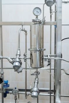
Membrane Filtration, including RO systems and Nanofiltration (NF), provides high arsenic rejection rates (95–99% for RO, 80–95% for NF) by size exclusion and charge repulsion. These technologies can effectively treat influent arsenic concentrations of 1–10 mg/L down to <0.01 mg/L. However, membranes are susceptible to fouling from co-contaminants like TMAH, silica, and suspended solids, necessitating robust pretreatment such as a DAF system for TSS and FOG removal in microelectronics wastewater. Ultrafiltration (UF) is often used as a pretreatment step before RO/NF.
Electrochemical Oxidation is an emerging technology that uses electrodes, such as boron-doped diamond (BDD) electrodes, to oxidize As(III) to As(V) and subsequently promote its removal through electrocoagulation or electro-adsorption. Pilot data show promising results, with up to 99% arsenic removal achieved at current densities of 10 mA/cm², offering a compact, chemical-free alternative.
AlAsO₄ Precipitation is a novel process demonstrating high efficiency in lab-scale studies. This method involves the controlled precipitation of aluminum arsenate (AlAsO₄) under acidic conditions (pH 3–5). Research indicates >99% arsenic removal, forming a stable, less soluble precipitate, potentially simplifying sludge management compared to traditional ferric precipitation.
Designing a Microelectronics Arsenic Treatment Train: Process Flow and Optimization
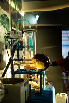
An effective microelectronics arsenic wastewater treatment train integrates multiple technologies to achieve stringent discharge limits and facilitate water reuse. A typical process flow for microelectronics arsenic wastewater treatment involves equalization, robust oxidation, pH adjustment, chemical precipitation, dissolved air flotation (DAF), membrane filtration (RO/NF), and polishing, often culminating in Zero Liquid Discharge (ZLD).Process Flow Diagram:
Equalization Tank → Oxidation (ClO₂/O₃) → pH Adjustment → Chemical Precipitation (Ferric Chloride) → Flocculation → Sedimentation (Lamella Clarifier) → DAF system for TSS and FOG removal in microelectronics wastewater → Ultrafiltration (UF) → RO system for arsenic removal and ultrapure water production → Polishing (AA/IX) → ZLD (Evaporation/Crystallization) → Sludge Dewatering (Filter Press)
Pretreatment:
- Equalization: Essential to buffer fluctuations in arsenic concentrations (e.g., 1–10 mg/L) and flow rates (e.g., 50–500 m³/h) from various fab processes. Equalization tanks are typically sized for a 2–4 hour hydraulic retention time (HRT) to ensure consistent influent quality for downstream units.
- Oxidation: The primary goal is to convert As(III) to As(V). Chlorine dioxide (ClO₂) at 1–2 mg/L or ozone (O₃) at 2–5 mg/L are highly effective, with typical contact times of 30 minutes. Reaction equations include H₃AsO₃ + ClO₂ → H₂AsO₄⁻ + ClO₂⁻ + H⁺ and H₃AsO₃ + O₃ → H₂AsO₄⁻ + O₂ + H⁺. Optimal pH for these reactions is generally 6–8.
- pH Adjustment: Following oxidation, pH is adjusted using lime (Ca(OH)₂) or sulfuric acid (H₂SO₄) to optimize conditions for subsequent treatment steps. For ferric chloride precipitation, a pH of 5–7 is ideal.
Primary Treatment:
- Chemical Precipitation: Ferric chloride (50–150 mg/L) or alum (100–200 mg/L) is dosed at the optimized pH of 5–7. This step involves rapid mixing for coagulant dispersion, followed by slow mixing in flocculation tanks (20–30 min HRT) to promote floc growth. Sedimentation in lamella clarifiers (20–40 m/h surface loading) effectively removes the formed arsenic-laden flocs.
- DAF: A DAF system is crucial to remove residual total suspended solids (TSS) and fats, oils, and grease (FOG) that can cause fouling in downstream membrane units. Typical parameters include an air-to-solids ratio of 0.02–0.05 and a loading rate of 5–10 m/h.
Secondary Treatment:
- Membrane Filtration: RO systems offer 95–99% arsenic rejection, while Nanofiltration (NF) achieves 80–95% rejection. Thin-film composite membranes are common. Typical membrane flux rates range from 15–25 LMH (liters per square meter per hour), with system recoveries often between 75–90%. Pretreatment is vital to mitigate fouling from TMAH, ammonia, and silica.
- Polishing: For achieving <0.01 mg/L arsenic or for specific water reuse applications, activated alumina (AA) or ion exchange (IX) can be used as polishing steps. AA typically requires regeneration every 10–20 bed volumes (BV), while IX resins require regeneration every 50–100 BV.
ZLD Integration:
- Evaporation/Crystallization: To achieve ZLD, concentrated RO brine is further treated using mechanical vapor recompression (MVR) or thermal evaporators/crystallizers. These systems typically consume 20–50 kWh/m³ and represent a significant CAPEX, ranging from $1M–$5M for a 100 m³/h brine treatment capacity.
- Sludge Dewatering: Arsenic-laden sludge from precipitation or evaporator blowdown is dewatered using a plate-and-frame filter press or centrifuge. A filter press can achieve 20–30% solids content, while centrifuges typically reach 15–25% solids, reducing sludge volume for disposal.
Zero Liquid Discharge (ZLD) for Microelectronics Arsenic Wastewater: Costs, ROI, and Case Studies
Cost Breakdown for a 100 m³/h ZLD System (Microelectronics Arsenic Wastewater):
| Cost Category | CAPEX Estimate | OPEX Estimate ($/m³) |
|---|---|---|
| Total System Cost | $3M–$5M | $3.00–$6.00 |
| Pretreatment (DAF, Chemical Dosing) | $500K–$800K | $0.20–$0.40 |
| RO/NF System | $1M–$1.5M | $0.50–$1.00 |
| Evaporator/Crystallizer (MVR/Thermal) | $1.5M–$2.5M | $1.50–$3.00 (energy-dominant) |
| Sludge Dewatering (Filter Press) | $200K–$400K | $0.10–$0.20 |
| Chemicals (Oxidants, Coagulants, Antiscalants) | N/A | $0.50–$1.00 |
| Membrane Replacement & Maintenance | N/A | $0.30–$0.50 |
| Sludge Disposal (Hazardous Waste) | N/A | $0.20–$0.50 |
| Labor & Other Utilities | N/A | $0.20–$0.40 |
Return on Investment (ROI) Calculation:
Implementing a ZLD system often demonstrates a compelling ROI by mitigating regulatory fines, reducing freshwater consumption, and eliminating off-site disposal costs. For example, a microelectronics fab currently paying $1.50/m³ for off-site wastewater disposal and facing $250K/year in fines for non-compliance could achieve an ROI in 3–5 years with a ZLD system. The benefits include reduced water intake costs (e.g., $1.00/m³ for freshwater), avoided discharge fees, and enhanced corporate environmental responsibility. Advanced RO systems are a core component of most ZLD solutions.Case Study 1: Semiconductor Fab in Taiwan (150 m³/h)
- Problem: Consistent arsenic exceedances (5–8 mg/L influent) and severe TMAH-induced fouling of existing RO membranes, leading to operational instability and regulatory penalties.
- Solution: Zhongsheng Environmental designed and implemented a ZLD treatment train comprising ozone oxidation, ferric chloride precipitation, a DAF system, a high-recovery RO system, and a mechanical vapor recompression (MVR) evaporator for brine concentration.
- Results: Achieved stable arsenic effluent concentrations of <0.01 mg/L, 92% water reuse rate, and eliminated discharge violations. The total CAPEX was approximately $4.2M, with an OPEX of $4.50/m³. The estimated ROI period was 4 years, driven by water savings and avoided fines.
Case Study 2: Solar Cell Manufacturer in China (50 m³/h)
- Problem: High concentrations of arsenic (10–15 mg/L) and fluoride (50–100 mg/L) in etching wastewater, requiring comprehensive treatment to meet stringent discharge and reuse standards. For a detailed look at related challenges, see our article on fluoride and arsenic treatment for solar cell wastewater.
- Solution: A treatment train combining lime precipitation for fluoride and initial arsenic removal, followed by activated alumina (AA) adsorption for polishing arsenic, Nanofiltration (NF) for further contaminant reduction, and a crystallizer for ZLD.
- Results: Arsenic concentrations reduced to <0.05 mg/L, fluoride to <5 mg/L, with an 85% water reuse rate. The project involved a CAPEX of $2.8M and an OPEX of $3.80/m³, demonstrating effective multi-pollutant removal with significant water conservation.
Global Compliance Standards for Arsenic in Microelectronics Wastewater: EPA, EU, and China Limits
Compliance with global discharge standards for arsenic is paramount for microelectronics facilities, as regulatory limits are becoming increasingly stringent and enforcement is intensifying. Designing a treatment system requires a clear understanding of local and international regulations.| Region/Country | Arsenic Discharge Limit (mg/L) | Enforcement Agency | Citation/Regulation |
|---|---|---|---|
| USA (EPA) | 0.1 | Environmental Protection Agency (EPA) | 40 CFR Part 469, Subpart A (Semiconductor Manufacturing) |
| EU | 0.1 | Member State Environmental Agencies | Industrial Emissions Directive (IED) 2010/75/EU (BAT-AEL for Semiconductor Manufacturing) |
| China | 0.1 | Ministry of Ecology and Environment (MEE) | GB 31573-2015 (Discharge Standard for Electronic Industry) |
| Taiwan | 0.05 | Environmental Protection Administration (EPA) | Effluent Standard for Semiconductor Industry |
| South Korea | 0.1 | Ministry of Environment (MOE) | Water Quality Standard for Industrial Wastewater |
Enforcement Trends:
- The U.S. EPA has significantly increased inspections of semiconductor fabs since 2020, with fines for arsenic violations potentially reaching up to $50K per day, reflecting a stricter enforcement posture (per EPA enforcement data).
- China’s Ministry of Ecology and Environment (MEE) now mandates online monitoring for arsenic in microelectronics wastewater discharges under GB 31573-2015, requiring real-time data submission to ensure continuous compliance.
- The EU’s Industrial Emissions Directive (IED) is driving towards Best Available Techniques (BAT) and, in water-stressed regions like Germany and the Netherlands, increasingly mandates ZLD for new semiconductor manufacturing facilities to minimize environmental impact.
Permitting Requirements:
- USA: Direct dischargers into surface waters require a National Pollutant Discharge Elimination System (NPDES) permit, which specifies arsenic limits. Indirect dischargers to Publicly Owned Treatment Works (POTWs) must meet pretreatment standards outlined in 40 CFR Part 403.
- EU: Facilities are required to obtain an IED permit, which includes a comprehensive assessment of Best Available Techniques (BAT) for arsenic treatment and sets specific emission limit values.
- China: New microelectronics fabs must undergo a rigorous Environmental Impact Assessment (EIA), where the design of arsenic wastewater treatment systems is thoroughly reviewed and approved by the MEE.
Frequently Asked Questions
Q: What is the most cost-effective arsenic treatment technology for microelectronics wastewater?
A: For influent arsenic concentrations below 5 mg/L, activated alumina (AA) or zero valent iron (ZVI) systems are generally the most cost-effective, with operational expenses (OPEX) ranging from $0.30–$1.00/m³. For higher arsenic concentrations (>5 mg/L) or when Zero Liquid Discharge (ZLD) is required, RO/NF systems become the preferred choice, despite higher capital expenditure (CAPEX), with OPEX typically $0.50–$2.00/m³. Chemical precipitation with ferric chloride is a low-CAPEX option but incurs significant ongoing costs for hazardous sludge disposal, as detailed in the treatment technology cost table above.
Q: How do I prevent arsenic from fouling RO membranes in microelectronics wastewater?
A: Effective membrane fouling prevention for arsenic in microelectronics wastewater relies on robust pretreatment. This includes comprehensive oxidation (e.g., chlorine dioxide or ozone) to convert all As(III) to As(V), followed by chemical precipitation (typically with ferric chloride) and a DAF system for TSS and FOG removal in microelectronics wastewater. These steps remove particulates and colloids that contribute to fouling. Maintaining a Silt Density Index (SDI) of <3 and turbidity of <0.1 NTU before the RO unit is critical. Additionally, the use of appropriate antiscalants (e.g., phosphonates) is essential to prevent silica and other mineral scaling on the membranes.
Q: What are the disposal requirements for arsenic-laden sludge from microelectronics wastewater treatment?
A: Arsenic-laden sludge from microelectronics wastewater treatment is typically classified as hazardous waste due to its toxicity. In the USA, it falls under EPA Hazardous Waste Code D004 and must be disposed of in a RCRA Subtitle C landfill, which is specifically engineered for hazardous waste. In the EU, it is classified as hazardous waste (EWC 06 07 01*) and requires secure landfill disposal or specialized incineration. China mandates stabilization (e.g., cement solidification) of arsenic sludge to reduce its leachability before it can be sent to designated hazardous waste landfills (per EPA PDF, Arsenic Treatment Technologies for Soil, Waste, and Water).
Q: Can I reuse treated microelectronics wastewater for ultrapure water production?
A: Yes, treated microelectronics wastewater can be reused for ultrapure water (UPW) production, but it requires an advanced, multi-stage treatment train. Effluent from RO systems, typically achieving <0.01 mg/L arsenic, serves as the feed for further polishing. This polishing often includes ion exchange (IX) or electrodeionization (EDI) to remove residual ions and achieve ultrapure water quality (resistivity >18 MΩ·cm). Critical pretreatment steps are necessary to ensure removal of co-contaminants like TMAH, ammonia, and silica, which can severely impact UPW system performance and membrane lifespan.
Q: What are the emerging technologies for arsenic removal in microelectronics wastewater?
A: Two promising emerging technologies for arsenic removal in microelectronics wastewater are electrochemical oxidation and AlAsO₄ precipitation. Electrochemical oxidation, often utilizing boron-doped diamond (BDD) electrodes, demonstrates high efficiency, achieving up to 99% arsenic removal at current densities around 10 mA/cm². This technology offers a compact footprint and reduced chemical consumption. AlAsO₄ precipitation is another novel approach that has shown >99% arsenic removal in lab-scale studies at an optimal pH range of 3–5, forming a stable precipitate. Both technologies are currently undergoing pilot testing for practical microelectronics applications, aiming to improve efficiency, reduce sludge volume, and lower operational costs compared to conventional methods.
Related Guides and Technical Resources
Explore these in-depth articles on related wastewater treatment topics: