Wastewater treatment expert: +86-181-0655-2851 Get Expert Consultation

Industry News

Silicon Wafer Wastewater Discharge Standards 2025: China GB vs Global Limits & Zero-Risk Compliance Blueprint

Silicon Wafer Wastewater Discharge Standards 2025: China GB vs Global Limits & Zero-Risk Compliance Blueprint
A sudden EPA inspection report landing on a fab manager’s desk, detailing non-compliance with effluent discharge limits, underscores the severe financial and operational risks posed by failing to meet silicon wafer wastewater discharge standards. Global regulations, while sharing core parameters like TSS (<10 mg/L), fluoride (<10 mg/L), and pH (6–9), present critical differences: China’s GB 8978-1996 mandates TSS ≤ 70 mg/L and fluoride ≤ 10 mg/L, whereas US EPA’s Effluent Guidelines (40 CFR Part 469) require stricter limits for semiconductor fabs, notably TSS ≤ 20 mg/L and fluoride ≤ 4 mg/L. Navigating these varied and stringent requirements demands advanced engineering solutions; hybrid Zero Liquid Discharge (ZLD) systems, integrating Dissolved Air Flotation (DAF), Membrane Bioreactors (MBR), and Reverse Osmosis (RO), are engineered to achieve over 99.8% TSS removal and <0.1 NTU turbidity, enabling not only compliance but also up to 30% water reuse, which is vital for fabs facing both escalating water scarcity and rigorous regulatory scrutiny.

Why Silicon Wafer Wastewater Fails Discharge Standards: The Hidden Compliance Risks

Colloidal silicon particles, often less than 1 μm in size, resist gravity settling due to their small mass and electrostatic surface charges, leading to persistent Total Suspended Solids (TSS) violations even with conventional clarifiers. During silicon wafer back grinding and dicing, sub-micron silicon fragments are released into the wastewater stream, forming stable colloidal suspensions. These particles possess a negative zeta potential in typical wastewater pH ranges, causing mutual repulsion and preventing agglomeration necessary for effective sedimentation. This inherent characteristic means that standard clarifiers, designed for larger, settleable solids, are fundamentally inadequate for achieving the low TSS limits mandated by modern discharge standards, leaving fabs vulnerable to compliance failures. the aggressive chemical agents used in wafer fabrication processes, such as piranha mixtures (concentrated H₂SO₄ + H₂O₂) for organic residue removal and hydrofluoric acid (HF) for oxide etching, generate highly acidic wastewater streams. Effluent pH levels frequently drop below 2, triggering immediate and automatic non-compliance with global pH discharge limits, which typically range from 6 to 9. This necessitates robust automated pH neutralization systems to prevent environmental damage and regulatory penalties. Fluoride is another critical contaminant, with concentrations from etching processes often exceeding local and international limits. For instance, influent fluoride can range from 100–500 mg/L, far surpassing China GB 8978-1996’s 10 mg/L and US EPA’s 4 mg/L limits for semiconductor effluent. Effective fluoride removal strategies for semiconductor wastewater, primarily calcium salt precipitation, are essential. A Taiwanese fab, as reported in industry data, achieved 99.9% fluoride removal, demonstrating the necessity of dedicated treatment stages. Finally, dissolved heavy metals such as copper (Cu), nickel (Ni), and chromium (Cr) from Chemical Mechanical Planarization (CMP) processes pose significant compliance challenges. These metals often exist in chelated forms, making conventional precipitation ineffective. EU Directive 2010/75/EU, for example, imposes stringent limits, often requiring concentrations below 0.5 mg/L for hazardous substances. Meeting these limits demands advanced treatment, including specific chelating agent breaking, robust membrane rejection (e.g., in RO systems), or ion exchange, to prevent environmental contamination and comply with strict TFT-LCD wastewater treatment solutions and broader semiconductor industry regulations.

Global Silicon Wafer Wastewater Discharge Standards: China GB vs US EPA, EU, and Taiwan Limits

Understanding the divergent global silicon wafer wastewater discharge standards is fundamental for semiconductor fabs operating across multiple jurisdictions, as compliance thresholds vary significantly. While a universal standard does not exist, key regulatory bodies and regions have established specific limits that dictate treatment requirements and operational strategies. The most prominent include China’s GB 8978-1996, US EPA’s 40 CFR Part 469, EU Directive 2010/75/EU, and Taiwan’s EPA regulations.

The following table provides a side-by-side comparison of critical parameters:

Parameter China GB 8978-1996 (Electronic Component Mfg.) US EPA 40 CFR Part 469 (Semiconductor Mfg.) EU Directive 2010/75/EU (Industrial Emissions Directive) Taiwan EPA (Semiconductor Industry)
TSS (mg/L) ≤ 70 ≤ 20 (Daily Max) Typically < 10 (Local Permit) ≤ 10 (Daily Average)
pH 6–9 6–9 6–9 6–9
Fluoride (mg/L) ≤ 10 ≤ 4 (Daily Max) Typically < 5 (Local Permit) ≤ 5
Total Nitrogen (mg/L) ≤ 15 No specific federal limit; local limits apply Typically < 10 (Local Permit) ≤ 20
Total Phosphorus (mg/L) ≤ 1 No specific federal limit; local limits apply Typically < 0.5 (Local Permit) ≤ 2
COD (mg/L) ≤ 100 No specific federal limit; local limits apply Typically < 100 (Local Permit) ≤ 100
BOD (mg/L) ≤ 20 No specific federal limit; local limits apply Typically < 20 (Local Permit) ≤ 30
Heavy Metals (Cu, Ni, Cr, As) (mg/L) Cu ≤ 0.5, Ni ≤ 1.0, Cr ≤ 0.5, As ≤ 0.1 Cu ≤ 0.5 (Daily Max) for some processes; local limits vary Typically < 0.1–0.5 for individual metals; zero discharge for hazardous substances (Local Permit) Cu ≤ 0.3, Ni ≤ 0.5, Cr ≤ 0.5, As ≤ 0.05
Oil & Grease (mg/L) ≤ 5 No specific federal limit; local limits apply Typically < 5 (Local Permit) ≤ 5
China’s GB 8978-1996, applying to ‘electronic component manufacturing’, sets a fluoride limit of 10 mg/L, which appears less stringent than the US EPA’s 4 mg/L daily maximum for ‘semiconductor manufacturing’ (NAICS 334413). However, local Chinese environmental protection bureaus often impose stricter regional limits, pushing effective compliance targets closer to international benchmarks. The EU Directive 2010/75/EU, while not providing uniform numerical limits, mandates the use of Best Available Techniques (BAT) to prevent or reduce emissions, often translating into near zero-discharge requirements for hazardous substances, driving ZLD adoption in European fabs. Taiwan’s EPA limits, particularly for TSS (≤10 mg/L) and fluoride (≤5 mg/L), are among the more rigorous globally. A notable case study from a Taiwanese fab demonstrated achieving TSS levels below 2 mg/L and turbidity below 0.1 NTU through advanced microfiltration, significantly exceeding all listed global standards. This performance sets a de facto benchmark for advanced fabs aiming for high-purity water reuse. While US EPA’s categorical limits in 40 CFR Part 469 specifically apply to "semiconductor manufacturing," China’s broader "electronic component manufacturing" classification under GB 8978-1996 means fabs must be vigilant in understanding how their specific operations are categorized and permitted locally.

Hybrid ZLD System Design for Silicon Wafer Wastewater: Engineering Specs for 99.8% TSS Removal

silicon wafer wastewater discharge standard - Hybrid ZLD System Design for Silicon Wafer Wastewater: Engineering Specs for 99.8% TSS Removal
Achieving 99.8% TSS removal and stringent effluent quality for silicon wafer wastewater typically relies on a multi-stage hybrid Zero Liquid Discharge (ZLD) system, meticulously designed with specific engineering parameters for each component. These systems leverage a combination of physical, chemical, and biological processes to handle the complex contaminant profile of semiconductor effluent, from colloidal silicon to dissolved metals and organics.

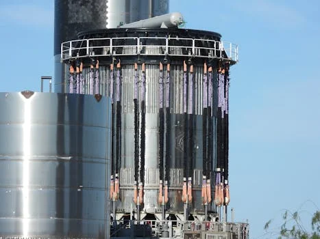
A typical hybrid ZLD system for silicon wafer wastewater includes the following stages:

Treatment Stage Primary Function Influent Specs (Typical) Effluent Specs (Target) Key Engineering Parameters
DAF Pre-treatment Colloidal Silicon, Oil & Grease Removal TSS: 50-150 mg/L (or up to 1100 NTU)
Oil & Grease: 10-50 mg/L
TSS: <50 NTU (<10 mg/L)
Oil & Grease: <5 mg/L
Air-to-Solids Ratio: 0.01-0.05
Retention Time: 20-30 min
Chemical Dosing: Coagulant (e.g., PAC), Flocculant (e.g., polymer)
pH Neutralization & Fluoride Precipitation pH Adjustment, Fluoride Removal pH: <2 or >10
Fluoride: 100-500 mg/L
pH: 6.5-8.5
Fluoride: <10 mg/L
Automated Ca(OH)₂ or CaCl₂ dosing
Reaction Time: 30-60 min
Sludge Production: High (CaF₂)
MBR Biological Stage COD, BOD, Ammonia Removal COD: 500-1500 mg/L
BOD: 100-300 mg/L
TSS: <50 mg/L (post-DAF)
COD: <50 mg/L (99% removal)
BOD: <10 mg/L
TSS: <2 mg/L (99.8% removal)
Turbidity: <0.1 NTU
Membrane Type: Submerged PVDF, 0.1 μm pore size
MLSS: 8,000-12,000 mg/L
Flux: 10-20 LMH
SRT: 20-40 days
RO Polishing TDS, Heavy Metal, Residual Ion Removal; Water Reuse TDS: 100-500 mg/L
Hardness: 50-150 mg/L
Silica: <50 mg/L
TDS: <10 mg/L
Hardness: <5 mg/L
Water Recovery: 75-85%
Two-stage configuration
Anti-scalant Dosing: Silica/Calcium control
Membrane Fouling Risk: Silica, organics
ZLD Integration (Evaporator/Crystallizer) Brine Volume Reduction RO Concentrate: 15-25% of influent volume Solid Waste: 1-2% of influent volume (for landfill) Energy Consumption: High (thermal)
Material Selection: Corrosion resistance
CAPEX/OPEX Trade-offs
DAF systems for colloidal silicon removal serve as the crucial pre-treatment stage. Micro-bubble flotation effectively removes up to 95% of colloidal silicon, oil, and grease. Influent TSS levels, which can be as high as 1100 NTU, are reduced to below 50 NTU in the effluent by optimizing the air-to-solids ratio and chemical dosing with coagulants and flocculants. This prevents downstream membrane fouling. Following pre-treatment, the MBR systems for semiconductor wastewater provide robust biological treatment and advanced solids separation. Submerged PVDF membranes with a 0.1 μm pore size achieve over 99% COD removal, transforming influent COD from 500–1500 mg/L to below 50 mg/L. Crucially, the MBR stage achieves 99.8% TSS removal, resulting in effluent turbidity often below 0.1 NTU, as highlighted by successful fab implementations. This high-quality effluent is ideal for subsequent membrane processes. For final polishing and water reuse, RO systems for zero liquid discharge compliance are deployed. Typically configured in two stages with anti-scalant dosing to mitigate membrane fouling from silica and organics, RO recovers 75–85% of the water, producing permeate with TDS levels below 10 mg/L. The concentrated brine from the RO system is then fed into ZLD integration units like crystallizers or evaporators, which further reduce concentrate volume by over 90%, enabling the disposal of solid waste to landfills and eliminating liquid discharge. While ZLD integration involves higher CAPEX and OPEX due to energy demands, it offers significant long-term benefits in water conservation and regulatory compliance.

Compliance Blueprint: Step-by-Step Risk Mitigation for Semiconductor Fabs

A robust compliance blueprint for semiconductor fabs integrates proactive pre-treatment, continuous monitoring, meticulous permitting, and accurate reporting to systematically mitigate the risks of wastewater discharge violations. Implementing these steps is critical for maintaining operational continuity and avoiding severe penalties. The first step is comprehensive **Pre-treatment**. Install dedicated pH neutralization tanks equipped with automated pH and fluoride dosing systems. These systems should target an effluent pH range of 6.5–8.5 to meet global standards. Simultaneously, integrate fluoride precipitation reactors, typically utilizing calcium chloride (CaCl₂) dosing at a molar ratio of 1.2:1 (Ca:F). This process is proven to reduce fluoride concentrations from hundreds of mg/L to below 1 mg/L, achieving up to 99.9% removal, a critical factor for meeting US EPA’s 4 mg/L limit. For colloidal silicon, dissolved air flotation (DAF) systems should be installed upstream to remove fine particles before biological treatment, preventing TSS excursions. Next, establish continuous **Monitoring** protocols. Deploy online TSS meters, such as the Hach Solitax, at key points in the treatment train, particularly post-MBR, to ensure effluent TSS remains below 2 mg/L. Integrate online fluoride sensors (e.g., Thermo Scientific Orion) and pH probes with 24/7 data logging capabilities. These sensors must be calibrated weekly to maintain accuracy. Establish alarm thresholds that trigger immediate alerts to operators if parameters approach non-compliance limits, allowing for proactive intervention before a violation occurs. For **Permitting**, semiconductor fabs must meticulously align their discharge permits with local regulatory limits. This involves a detailed understanding of whether the facility falls under broader 'electronic component manufacturing' (like China’s GB 8978-1996) or specific 'semiconductor manufacturing' categorical limits (like US EPA’s 40 CFR Part 469). Permits should include comprehensive contingency plans for potential exceedances, such as emergency storage tanks to hold off-spec wastewater for re-treatment, preventing direct discharge of non-compliant effluent. Regular engagement with local environmental authorities is essential to stay updated on evolving regulations and permit requirements. Finally, implement automated **Reporting** systems. Monthly discharge reports must be generated with lab-certified data for all required parameters, including TSS, pH, fluoride, COD, BOD, and heavy metals (Cu, Ni, Cr). These reports should be submitted promptly via local EHS portals, such as China’s National Pollutant Discharge Permit System. Automating data collection and report generation minimizes human error, ensures data integrity, and streamlines the compliance process, providing a verifiable audit trail for regulatory bodies.

Cost-Optimized Equipment Selection: CAPEX, OPEX, and ROI for Hybrid ZLD Systems

silicon wafer wastewater discharge standard - Cost-Optimized Equipment Selection: CAPEX, OPEX, and ROI for Hybrid ZLD Systems
Strategic equipment selection for hybrid Zero Liquid Discharge (ZLD) systems in silicon wafer fabs requires a comprehensive analysis of Capital Expenditure (CAPEX), Operational Expenditure (OPEX), and Return on Investment (ROI) to ensure long-term cost optimization and compliance. The initial investment in advanced wastewater treatment can be substantial, but the long-term savings from water reuse and avoided penalties often justify the outlay.

A typical CAPEX breakdown for a 500 m³/day hybrid ZLD system in a semiconductor fab is as follows:

Equipment Category Estimated CAPEX Range (USD) Key Components
DAF System $150,000 – $300,000 Flotation tank, air saturation system, chemical dosing, sludge scraper
MBR System $200,000 – $500,000 Membrane modules, aeration system, pumps, controls
RO System $100,000 – $250,000 RO membranes, high-pressure pumps, anti-scalant dosing, CIP system
ZLD (Evaporator/Crystallizer) $500,000 – $1,200,000+ Thermal evaporator, crystallizer, heat exchangers, sludge dewatering
Ancillary Systems $50,000 – $200,000 Tanks, pumps, piping, instrumentation, control systems, pH neutralization
Total Estimated CAPEX (500 m³/day) $1,000,000 – $2,450,000
The CAPEX for a 500 m³/day hybrid ZLD system can range from $1 million to over $2.45 million, depending on the specific technologies and level of automation. For example, a Taiwanese fab mentioned in industry reports invested significantly in a system capable of 432 m³/day reuse, highlighting the scale of these projects. Operational Expenditure (OPEX) is primarily driven by energy consumption, membrane replacement, and chemical dosing. Energy costs typically range from 0.8–1.2 kWh/m³ for a complete hybrid ZLD system, with thermal evaporators being the most energy-intensive component. Membrane replacement for MBR and RO systems occurs every 3–5 years, representing a significant recurring cost. Chemical dosing for coagulation, flocculation, pH adjustment, and anti-scalants can add $0.10–$0.30/m³ to OPEX. Cost-saving strategies include optimizing chemical dosages, implementing energy recovery systems, or exploring innovative pre-treatment methods like solar-powered electrocoagulation to reduce chemical consumption. Return on Investment (ROI) for hybrid ZLD systems is compelling when considering both water reuse savings and avoided regulatory fines. For a 1000 m³/day fab, annual water reuse savings can amount to $182,500 – $730,000 (assuming $0.50–$2.00/m³ for raw water). Avoiding a single major regulatory violation, which can incur fines of $10,000–$50,000 per violation (or up to 1M RMB in China), further strengthens the ROI. A typical hybrid ZLD system can achieve payback within 3–5 years, driven by these combined savings and risk mitigation. When selecting a vendor, prioritize suppliers with proven semiconductor-specific case studies, such as the 432 m³/day reuse project in Taiwan, demonstrating direct experience with the unique challenges of silicon wafer wastewater. Evaluate vendors based on their ability to conduct on-site pilot testing, which provides critical data on membrane fouling resistance (especially for silica and organics), chemical consumption, and overall system performance tailored to the fab’s specific wastewater profile. This due diligence ensures the selected system is robust, efficient, and cost-effective for long-term compliance.

Frequently Asked Questions

Addressing common inquiries regarding silicon wafer wastewater discharge standards and treatment technologies is crucial for semiconductor fabs seeking clarity on compliance and engineering solutions. What is the TSS limit for silicon wafer wastewater in China? China’s GB 8978-1996 sets a TSS limit of 70 mg/L for electronic component manufacturing, but fabs often target <10 mg/L to align with US EPA and EU standards, and to facilitate high-purity water reuse. How do hybrid ZLD systems reduce fluoride levels to meet US EPA limits? Hybrid systems use calcium salt precipitation (e.g., CaCl₂ or Ca(OH)₂) to reduce fluoride from high influent concentrations (100–500 mg/L) to <4 mg/L, followed by reverse osmosis (RO) polishing to achieve even lower levels, often <1 mg/L, for discharge or reuse. What are the penalties for violating silicon wafer wastewater discharge standards? Penalties vary by jurisdiction: China imposes fines up to 1M RMB ($140K) and can mandate production halts or facility closures, while US EPA violations under the Clean Water Act can exceed $50K/day, alongside potential criminal charges for egregious non-compliance. Can MBR systems handle the high turbidity of silicon wafer wastewater? Yes, submerged PVDF MBR membranes with a 0.1 μm pore size can effectively handle influent turbidity up to 1100 NTU, achieving exceptional effluent quality with turbidity typically <0.1 NTU and over 99.8% TSS removal, as demonstrated in various fab applications. What monitoring equipment is required for semiconductor wastewater compliance? Mandatory equipment for real-time compliance monitoring includes online TSS meters, pH sensors, fluoride analyzers, flow meters, and COD/BOD sensors, all integrated with 24/7 data logging capabilities and automated alarm thresholds.

Related Articles

Photovoltaic Developer Wastewater Treatment: 2025 Engineering Specs, 99.9% Removal & Solar-Powered ZLD Cost Breakdown
Jun 1, 2026

Photovoltaic Developer Wastewater Treatment: 2025 Engineering Specs, 99.9% Removal & Solar-Powered ZLD Cost Breakdown

Discover 2025 engineering solutions for photovoltaic developer wastewater treatment—detailed proces…

Data Center Cooling Water Treatment Case Study: 40% Water Savings with Hybrid ZLD & RO System
Jun 1, 2026

Data Center Cooling Water Treatment Case Study: 40% Water Savings with Hybrid ZLD & RO System

Discover how a 200 MW data center reduced cooling water consumption by 40% using hybrid ZLD and RO …

How Dissolved Air Flotation (DAF) Systems Work: Engineering Process, Efficiency Data & Industrial Selection Guide 2025
Jun 1, 2026

How Dissolved Air Flotation (DAF) Systems Work: Engineering Process, Efficiency Data & Industrial Selection Guide 2025

Discover how dissolved air flotation (DAF) systems remove 95%+ TSS, FOG, and metals from industrial…

Contact
Contact Us
Call Us
+86-181-0655-2851
Email Us Get a Quote Contact Us