Semiconductor wastewater recycling reduces fab water consumption by 40-60% and cuts discharge costs by up to 30%, according to 2024 industry benchmarks. Specialized treatment is essential for key contaminants such as hydrofluoric acid (HF), ammonium hydroxide (NH4OH), and dissolved metals; for instance, MBR systems achieve 99.9% TSS removal, and RO membranes recover 75-90% of wastewater for reuse. This comprehensive guide provides engineering specifications, detailed cost breakdowns, and a practical decision framework to assist fab managers and engineers in selecting the optimal semiconductor wastewater recycling solution for their facility's unique waste stream complexity and budget.
Why Semiconductor Fabs Are Turning to Wastewater Recycling in 2025
Global semiconductor manufacturing consumes 2-4 million gallons of water per day per fab, creating immense pressure on freshwater resources and discharge infrastructure (per SEMI 2023 data). This escalating demand, coupled with increasing water scarcity in key manufacturing regions, is driving a critical shift towards advanced wastewater recycling solutions. Regulatory drivers, such as the EU Industrial Emissions Directive 2010/75/EU, EPA Effluent Limitation Guidelines (ELGs), and ambitious local mandates like Taiwan’s 2025 water reuse targets, compel fabs to minimize discharge and maximize water reuse. Beyond compliance, significant cost savings motivate these investments; recycling water can cost $0.50–$2.00 per 1,000 gallons, a substantial reduction compared to the $3.00–$5.00 per 1,000 gallons for freshwater acquisition and discharge (2024 industry averages). For example, TSMC’s 2023 water recycling initiative successfully reduced consumption by 30% across five fabs, demonstrating the tangible benefits of adopting robust semiconductor fab water reuse strategies (source: TSMC Sustainability Report 2023).
Semiconductor Wastewater Contaminants: Engineering Profiles and Treatment Challenges
semiconductor wastewater recycling - Semiconductor Wastewater Contaminants: Engineering Profiles and Treatment Challenges
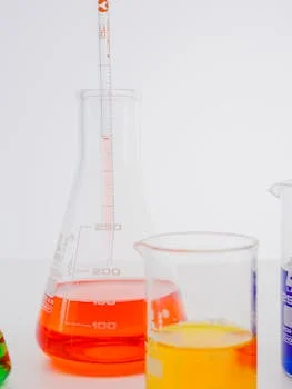
Semiconductor wastewater streams present a complex mix of acids, bases, metals, and organics, each demanding specific engineering approaches for effective treatment and recycling. Etching, cleaning, and chemical mechanical planarization (CMP) processes introduce a diverse array of contaminants. Hydrofluoric acid (HF), often present at 0.5–5% concentration, requires careful neutralization and specialized materials to prevent corrosion. Sulfuric acid (H2SO4, 10–98%) and ammonium hydroxide (NH4OH, 1–10%) are also common, necessitating precise pH adjustment to mitigate environmental impact and protect downstream equipment.
Dissolved metals like copper (Cu), nickel (Ni), and arsenic (As) are regulated by strict EPA ELG limits, typically requiring removal to below 0.5 mg/L for Cu and 1.0 mg/L for Ni. These metals often precipitate as hydroxides or sulfides, requiring robust separation. Organic solvents such as isopropyl alcohol (IPA), N-methyl-2-pyrrolidone (NMP), and acetone, while volatile, can inhibit biological treatment processes and may require advanced oxidation or distillation. Suspended solids, including silica and photoresist residues with particle sizes ranging from 0.1–100 μm, significantly contribute to membrane fouling if not effectively removed during pre-treatment. Emerging contaminants like tetramethylammonium hydroxide (TMAH), a common photoresist developer, pose unique challenges due to their toxicity and resistance to conventional biological treatment, often necessitating advanced oxidation processes or specialized resins. For effective treatment of challenging contaminants like TMAH, understanding the role of advanced oxidation, such as that provided by chlorine dioxide generators, is crucial.
Contaminant Class
Specific Contaminant
Typical Concentration/Range (Raw Wastewater)
Key Treatment Challenge
Target Removal Efficiency
Acids/Bases
Hydrofluoric Acid (HF)
0.5 – 5%
Corrosion, Toxicity, Requires neutralization
>99% (to near neutral pH)
Acids/Bases
Ammonium Hydroxide (NH4OH)
1 – 10%
pH adjustment, Ammonia stripping/nitrification
>95% (as NH3-N)
Dissolved Metals
Copper (Cu)
1 – 50 mg/L
Precipitation, EPA ELG (<0.5 mg/L)
>99%
Dissolved Metals
Nickel (Ni)
0.5 – 20 mg/L
Precipitation, EPA ELG (<1.0 mg/L)
>99%
Organics
Isopropyl Alcohol (IPA)
100 – 10,000 mg/L
Biodegradability, COD loading
>90% (as COD)
Organics
Tetramethylammonium Hydroxide (TMAH)
10 – 1,000 mg/L
Toxicity, Resistance to biological treatment, Advanced Oxidation required
>95% (as COD/TOC)
Suspended Solids
Silica, Photoresist Residues
50 – 500 mg/L (TSS)
Membrane fouling, Particle size (0.1-100 μm)
>99% (as TSS)
Wastewater Recycling Technologies: Engineering Specs and Performance Data
Advanced wastewater recycling technologies, including DAF, MBR, RO, and chemical dosing, offer distinct engineering specifications and performance capabilities crucial for meeting semiconductor fab water reuse targets. Each technology plays a specific role, often integrated into a multi-stage treatment train to achieve desired water quality.
Dissolved Air Flotation (DAF) systems, such as the Zhongsheng ZSQ series, are highly effective for pre-treatment of high-solids streams, achieving 90–95% TSS removal and 80–90% FOG (Fats, Oils, and Grease) removal. DAF pre-treatment for semiconductor wastewater is ideal for managing influent with significant suspended solids, colloids, and oil content, protecting downstream membrane systems from fouling.
Membrane Bioreactor (MBR) systems, like Zhongsheng's DF series, combine biological treatment with membrane filtration, offering superior effluent quality. These systems typically utilize 0.1 μm pore size membranes, achieving 99.9% TSS removal and 90–95% COD removal. MBR systems for semiconductor wastewater recycling are particularly suitable for biologically treating organic contaminants while providing a robust barrier against suspended solids and pathogens. Detailed MBR membrane pore sizes and flux rates for semiconductor applications are critical for optimal design.
Reverse Osmosis (RO) is a cornerstone technology for ultra-pure water recovery. Industrial RO system specs indicate 95–99% ion rejection, crucial for removing dissolved salts and heavy metals, and achieve 75–90% water recovery rates. RO systems for ultra-pure water reuse in fabs are indispensable for producing water that meets stringent semiconductor manufacturing standards. Understanding RO membrane rejection rates for semiconductor contaminants is key to achieving high-quality permeate.
Chemical Dosing Systems ensure precise control over water chemistry. Automatic dosing systems enable precise pH adjustment (typically ±0.1 pH units), crucial for neutralization and optimizing metal precipitation reactions using coagulants and flocculants. These systems are vital for primary treatment and conditioning water for subsequent membrane processes.
Electrocoagulation (EC) offers an alternative for heavy metal and suspended solids removal, achieving 95%+ heavy metal removal without requiring chemical additives. EC operates by introducing an electrical current (e.g., 5-20V, 5-200 A/m²) to sacrificial electrodes, generating coagulants in situ that destabilize contaminants for easier separation.
Technology
Key Application
Engineering Specs / Parameters
Typical Performance Data (Removal)
Advantages for Semiconductor Fabs
Dissolved Air Flotation (DAF)
Pre-treatment for high TSS/FOG streams
Hydraulic Loading: 1-3 m³/m²h; Air Saturation Pressure: 4-6 bar
Optimizes metal precipitation, enhances flocculation for TSS removal
Precise control, adaptable to variable waste streams, critical for multi-stage systems
Electrocoagulation (EC)
Heavy metal removal, COD/BOD reduction
Voltage: 5-20V; Current Density: 5-200 A/m²; Electrode Material: Fe/Al
95%+ Heavy Metals, 50-80% COD/BOD
No chemical addition for coagulation, compact, lower sludge volume
How to Match Recycling Technology to Your Fab’s Waste Stream
semiconductor wastewater recycling - How to Match Recycling Technology to Your Fab’s Waste Stream
Selecting the appropriate wastewater recycling technology for a semiconductor fab depends on a detailed assessment of waste stream complexity, available footprint, energy consumption, and target water quality. A "waste stream complexity matrix" helps categorize influent: simple streams primarily contain acids/bases, while complex streams include metals, organics, and challenging emerging contaminants like TMAH. For simple streams, a basic neutralization and filtration system might suffice for non-critical reuse. However, complex streams demand a multi-barrier approach.
Footprint constraints are a significant factor in space-limited fabs. MBR systems, for example, can be up to 60% smaller than conventional activated sludge systems for the same capacity due to the high biomass concentration and integrated filtration. DAF offers a compact pre-treatment solution, requiring less space than traditional clarifiers. Energy consumption also varies considerably; RO systems typically consume 3–5 kWh/m³ due to high-pressure pumps, while MBR systems operate at 0.5–1.5 kWh/m³, and electrocoagulation ranges from 2–4 kWh/m³. These energy costs directly impact operational expenditure.
Finally, the required water quality dictates the final technology stack. For ultra-pure water (UPW) reuse in critical process applications, a robust system including MBR, RO, and potentially EDI (Electrodeionization) is essential. For non-critical applications like cooling tower makeup or general utility water, MBR effluent might be sufficient. For example, a global semiconductor manufacturer faced a complex waste stream containing high concentrations of HF, heavy metals, and TMAH. Their custom system integrated a DAF pre-treatment, followed by a specialized MBR for organic and suspended solids removal, and then a multi-stage RO system with advanced oxidation pre-treatment for TMAH and final polishing, achieving 85% water recovery for process reuse.
Cost-effective for pH adjustment and basic solids removal for non-critical reuse.
Moderate
Acids/Bases, Metals, Moderate Organics, TSS
DAF + Chemical Precipitation + MBR
DAF for solids/metals, chemical precipitation for specific metals, MBR for biological treatment and advanced solids removal.
High
HF, Metals, IPA, NMP, TMAH, High TSS/COD
DAF + Chemical Precipitation + MBR + Advanced Oxidation + RO + EDI
Comprehensive treatment for diverse, recalcitrant contaminants to achieve ultra-pure water quality for critical process reuse.
Space-Constrained
Any Complexity
Compact DAF, Submerged MBR, Containerized RO
Optimized designs reduce physical footprint, crucial for existing fabs with limited expansion space.
Cost Breakdown: CAPEX, OPEX, and ROI for Semiconductor Wastewater Recycling
Implementing semiconductor wastewater recycling systems involves CAPEX ranging from $500K–$5M for systems handling 50–500 m³/h, with OPEX driven by membrane replacement, energy, and chemical consumption (2025 industry averages). Initial capital expenditure (CAPEX) covers equipment purchase, installation, civil works, and engineering. For a typical 200 m³/h system, CAPEX can range from $1.5M to $3M, depending on the complexity of the required technology stack and automation level.
Operational expenditure (OPEX) is a critical factor in long-term financial planning. Membrane replacement is a significant OPEX driver, with RO membranes typically lasting 3–5 years and MBR membranes 5–7 years. Energy costs are substantial, particularly for RO systems at $0.30–$0.50/m³, while MBR systems are more energy-efficient at $0.10–$0.20/m³, and electrocoagulation falls in the $0.20–$0.40/m³ range. Chemical consumption for pH adjusters, coagulants, and membrane cleaning agents also contributes significantly to OPEX.
The return on investment (ROI) for semiconductor wastewater recycling is often compelling, with payback periods typically ranging from 2–5 years. This ROI is primarily driven by substantial water savings (reducing freshwater acquisition costs) and avoidance of discharge fees. For example, a 200 m³/h system recycling 80% of its wastewater could save a fab approximately $1.5M annually in combined water purchase and discharge costs, leading to a payback period of under 3 years for a $3M system. Hidden costs, such as extensive pre-treatment requirements (e.g., DAF before RO), sludge disposal, and potential system downtime for maintenance, must be factored into the overall financial model. government grants and subsidy programs for water reuse, such as Taiwan’s 2025 subsidy program or EU Horizon Europe funding, can significantly improve ROI and accelerate adoption.
Cost Category
Typical Range/Driver (2025 Industry Averages)
Notes for Fab Managers
CAPEX (System Installation)
$500K – $5M (for 50-500 m³/h systems)
Includes equipment, engineering, civil works, installation. Varies significantly with automation level and technology complexity.
OPEX (Membrane Replacement)
RO: $0.05 – $0.15/m³ (3-5 year lifespan)
MBR: $0.03 – $0.08/m³ (5-7 year lifespan)
Consider membrane fouling rates, pre-treatment effectiveness, and cleaning protocols.
Varies with influent quality and required chemical dosing for semiconductor wastewater treatment.
Hidden Costs
Sludge disposal: $50-$200/ton; Pre-treatment upgrades; System downtime
Account for all ancillary costs beyond core system operation. Sludge volume and hazardous nature impact disposal costs.
ROI (Payback Period)
2 – 5 years
Calculated based on avoided freshwater purchase costs and reduced wastewater discharge fees. Incentives can shorten this period.
Implementation Checklist: 8 Steps to Deploy a Semiconductor Wastewater Recycling System
semiconductor wastewater recycling - Implementation Checklist: 8 Steps to Deploy a Semiconductor Wastewater Recycling System
Successfully deploying a semiconductor wastewater recycling system requires a systematic 8-step approach, beginning with detailed waste stream characterization and concluding with rigorous performance validation. Adhering to this structured process minimizes risks and ensures optimal system performance.
Step 1: Waste Stream Characterization – Conduct comprehensive sample analysis for pH, TSS, COD, BOD, specific metals (Cu, Ni, As), organics (IPA, NMP, TMAH), fluoride, and ammonia. This defines the exact contaminant profile and variability.
Step 2: Regulatory Compliance Review – Thoroughly understand all applicable regulations, including EPA ELGs for specific pollutants, local discharge limits, and water reuse standards (e.g., ISO 30500 for non-sewered systems or specific fab internal UPW standards).
Step 3: Technology Selection – Based on characterization and compliance needs, select appropriate technologies. Conduct pilot testing for MBR, RO, or hybrid systems for 3-6 months to validate performance with actual fab wastewater, ensuring success criteria like contaminant removal and water recovery rates are met.
Step 4: System Design – Develop detailed engineering designs, considering footprint constraints, redundancy for critical components, and automation requirements, such as PLC-controlled precise chemical dosing for semiconductor wastewater treatment and remote monitoring capabilities.
Step 5: Vendor Evaluation – Select a supplier based on proven semiconductor industry experience, modular construction capabilities (for faster deployment), comprehensive after-sales support, and a strong track record of delivering robust, reliable systems.
Step 6: Installation and Commissioning – Plan for a typical timeline of 6–12 months for a 200 m³/h system, including off-site fabrication and on-site assembly. Ensure rigorous safety protocols are in place throughout the installation phase.
Step 7: Operator Training – Provide comprehensive training for fab personnel on system operation, routine maintenance, troubleshooting, and certification requirements for handling hazardous chemicals (e.g., HF, NH4OH) safely.
Step 8: Performance Validation – After commissioning, conduct post-installation testing over several weeks to validate contaminant removal efficiencies, water quality metrics, and overall system stability against design specifications and regulatory limits.
Frequently Asked Questions
Fab managers and engineers frequently inquire about the complexities, benefits, and regulatory landscape surrounding semiconductor wastewater recycling, seeking clear, data-backed answers. This section addresses common concerns for semiconductor wastewater recycling.
What is the biggest challenge in recycling semiconductor wastewater?
The biggest challenge lies in the extreme variability of waste stream composition and the presence of highly persistent or proprietary chemicals, such as TMAH or specific photoresist components, which resist conventional biological and physical-chemical treatments. This necessitates highly adaptable and often multi-stage advanced treatment processes.
How much water can a semiconductor fab recycle?
A semiconductor fab can typically recycle 40–60% of its total water usage, depending on the sophistication of the recycling technology implemented, the complexity of the waste streams, and the quality requirements for the recycled water. Some advanced facilities can achieve even higher rates.
What are the maintenance requirements for a semiconductor wastewater recycling system?
Maintenance requirements typically include weekly membrane cleaning (e.g., chemical enhanced backwash for MBR, CIP for RO), daily calibration of chemical dosing systems, monthly sludge disposal, and regular checks of pumps, instrumentation, and control systems. Predictive maintenance based on sensor data is becoming increasingly common.
Can recycled water be used for ultra-pure water (UPW) production?
Yes, recycled water can be treated to meet ultra-pure water (UPW) standards, but it requires a comprehensive treatment train including MBR, multiple stages of RO, and often Electrodeionization (EDI) or mixed-bed ion exchange to achieve the required resistivity (typically 18 MΩ·cm) and low particle count.
What are the regulatory risks of not recycling semiconductor wastewater?
Fabs that do not implement robust semiconductor wastewater recycling face significant regulatory risks, including substantial fines for exceeding discharge limits (e.g., $25K–$100K per violation under EPA ELGs), potential reputational damage, and operational restrictions due to water supply limitations in drought-prone regions.
Our team of wastewater treatment engineers has over 15 years of experience designing and manufacturing DAF systems, MBR bioreactors, and packaged treatment plants for clients in 30+ countries worldwide.