Why Microelectronics Wastewater Standards Are Changing in 2025
Microelectronics wastewater discharge standards are tightening globally in 2025, with China’s GB8978-2025 draft imposing limits of 0.1 mg/L for arsenic, 0.5 mg/L for copper, and 1 mg/L for TMAH—stricter than EPA’s 40 CFR Part 469 (e.g., 1 mg/L arsenic) and the EU’s Industrial Emissions Directive (2010/75/EU). Zero-liquid-discharge (ZLD) systems, combining reverse osmosis (RO) and membrane distillation, achieve 98%+ recovery but require CAPEX of $2–5M for a 1,000 m³/day fab. Compliance hinges on hybrid treatment processes tailored to pollutant profiles, such as advanced oxidation for TMAH and selective ion exchange for heavy metals.
The urgency for these regulatory shifts stems from the massive expansion of 300mm wafer fabrication facilities across Asia and the increasing complexity of chemical mechanical planarization (CMP) and etching chemistries. In China, the upcoming GB8978-2025 revision (integrated with the GB 39731-2020 electronic industry standards) introduces a "dual control" system that monitors both total pollutant load and concentration. This is a direct response to the environmental strain in high-density tech hubs like the Yangtze River Delta, where cumulative heavy metal discharge has historically outpaced the self-purification capacity of local water bodies.
In the United States, while the EPA’s 40 CFR Part 469 (Semiconductor Manufacturing Point Source Category) remains the baseline, enforcement has intensified following the EPA 2023 memorandum regarding PFAS (per- and polyfluoroalkyl substances). Fabs are now under increased scrutiny to monitor "Total Toxic Organics" (TTO) more granularly. Similarly, the European Commission’s 2024 guidance on the Industrial Emissions Directive (IED) now classifies the microelectronics sector as a "high-risk sector" for heavy metal pollution, mandating the adoption of Best Available Techniques (BAT) to minimize the discharge of nickel, chromium, and copper.
The financial risks of non-compliance are no longer theoretical. In 2023, TSMC’s operations in Taiwan faced a fine equivalent to approximately $10M following chromium exceedances detected in local water systems, highlighting the vulnerability of even the most technologically advanced fabs to EHS (Environmental, Health, and Safety) oversight. As fab expansion moves into water-scarce regions of Southeast Asia, such as Vietnam and India, local authorities are increasingly bypassing conventional discharge permits in favor of mandatory on-site ZLD adoption to protect limited groundwater resources.
Global Microelectronics Wastewater Discharge Standards Compared: China GB8978 vs EPA vs EU
Global regulatory frameworks for microelectronics wastewater are diverging in their specific pollutant limits, with China’s 2025 standards emerging as some of the most stringent for specific semiconductor-grade chemicals like TMAH. While the EPA focuses on TTO and fluoride, China’s GB8978-2025 draft targets the high-toxicity profiles of modern photoresist developers and CMP slurries. Understanding these variations is critical for EHS managers operating international fab portfolios.
| Pollutant Parameter | China GB8978-2025 (Draft/IC Spec) | EPA 40 CFR Part 469 (US) | EU IED 2010/75/EU (BAT Limits) | Unit |
|---|---|---|---|---|
| Arsenic (As) | 0.1 | 1.0 | 0.15 | mg/L |
| Copper (Cu) | 0.5 | 0.5 (Average) | 0.5 | mg/L |
| Total Chromium (Cr) | 0.5 | 1.0 (TTO proxy) | 0.2 | mg/L |
| Nickel (Ni) | 0.1 | N/A (Local limits apply) | 0.5 | mg/L |
| TMAH | 1.0 | Not Explicitly Regulated | Not Explicitly Regulated | mg/L |
| Fluoride (F-) | 10.0 | 17.4 (Daily Max) | 15.0 | mg/L |
| Ammonium (NH4-N) | 10.0 | N/A | 15.0 - 20.0 | mg/L |
| Total Suspended Solids (TSS) | 30.0 | N/A (Local limits apply) | 35.0 | mg/L |
A significant gap in global standards is the regulation of Tetramethylammonium hydroxide (TMAH). China’s GB8978-2025 includes a strict 1 mg/L limit for TMAH, whereas the EPA and EU do not explicitly regulate it under federal/central law, often leaving it to regional municipal pretreatment requirements. However, the World Health Organization (WHO) 2022 guidelines on TMAH toxicity emphasize its acute neurological and dermal risks, which is driving a push for voluntary ESG compliance among US and European manufacturers.
Local enforcement mechanisms also differ significantly. China utilizes a "dual control" system where fabs must meet both concentration limits and a total annual mass load (Total Load Control). In contrast, the US EPA primarily relies on "technology-based" limits (Best Available Technology Economically Achievable), though "water-quality-based" limits may be imposed if a fab discharges into a sensitive watershed. In water-stressed regions like Singapore (NEA requirements) and Israel, "zero-discharge" is often a prerequisite for obtaining a construction permit for new 12-inch wafer facilities.
Key Pollutants in Microelectronics Wastewater: Toxicity, Sources, and Treatment Challenges
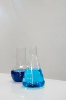
The complexity of microelectronics wastewater arises from the co-existence of high-concentration organic developers and trace-level inorganic heavy metals, each requiring distinct removal mechanisms. Standard biological treatment is often insufficient due to the inhibitory nature of semiconductor chemicals on microbial activity. To meet 2025 standards, engineers must address the specific chemical properties of these pollutants.
Tetramethylammonium hydroxide (TMAH): Primarily used in the photoresist development process, TMAH is highly toxic to aquatic life even at concentrations as low as 0.5 mg/L. It behaves as a strong base and a quaternary ammonium cation, making it resistant to standard aerobic digestion. Successful removal typically requires advanced oxidation processes (AOPs), such as UV/H₂O₂ or ozone, followed by specialized biological treatment using Nitrosomonas bacteria for nitrification. Achieving 99%+ removal efficiency is necessary to meet the 1 mg/L threshold in China’s 2025 draft.
Heavy Metals (As, Cr, Cu): Arsenic originates from CMP slurries and ion implantation, while chromium and copper are byproducts of etching and plating. Hexavalent chromium (Cr⁶⁺) is of particular concern, as it is roughly 100 times more toxic than Cr³⁺ and is strictly regulated under EPA IRIS guidelines. Treatment involves a multi-stage process: reduction of Cr⁶⁺ to Cr³⁺ using sodium bisulfite, followed by hydroxide precipitation and engineering specs for arsenic removal in microelectronics wastewater that utilize selective ion exchange resins to achieve sub-ppb levels.
Ammonium and Fluoride: Ammonium is a byproduct of TMAH degradation and can lead to rapid eutrophication if discharged. It is typically managed through biological nitrification/denitrification or chemical struvite precipitation. Fluoride, resulting from hydrofluoric acid (HF) etching, is regulated at 10 mg/L (China) versus 4 mg/L (EPA drinking water standards). The standard treatment involves calcium chloride precipitation to form calcium fluoride (CaF₂) sludge, followed by adsorption with activated alumina for polishing.
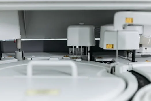
Zero-Liquid-Discharge (ZLD) Systems for Microelectronics: Engineering Specs and Cost Breakdown
Transitioning to a ZLD model allows IC fabs to achieve 98% water recovery, virtually eliminating discharge risk while securing a stable supply of process water. A robust ZLD system for microelectronics is a hybrid configuration that balances energy consumption with the need to handle high-Total Dissolved Solids (TDS) streams. The design must account for the high silica content typical of semiconductor wastewater, which can lead to rapid membrane scaling.
| Treatment Stage | Technology Employed | Recovery Rate | Energy Intensity (kWh/m³) |
|---|---|---|---|
| Pre-treatment | pH Adjust / DAF / Softening | 98% (Volume) | 0.2 - 0.5 |
| Primary Recovery | High-Rejection RO | 75% - 85% | 1.2 - 2.5 |
| Brine Concentration | Membrane Distillation (MD) | 85% - 92% | 15.0 - 20.0 |
| Final Solidification | Mechanical Vapor Recompression (MVR) | 99%+ | 30.0 - 50.0 |
For a 1,000 m³/day fab, the CAPEX for a full ZLD system is substantial. A typical breakdown includes $2M for RO systems for microelectronics wastewater recovery, $1.5M for membrane distillation or electrodialysis (ED) units, and $1M for the final crystallizer. Automation and real-time analytical suites add approximately $500K. Despite the high initial cost, the OPEX remains manageable at $0.50–$1.20/m³ when factoring in reduced raw water procurement costs and the avoidance of discharge fines.
Real-world implementation, such as Intel’s Chandler, AZ facility, demonstrates that ZLD system design and cost breakdown for IC fabs can lead to a 30% reduction in overall water-related operational costs. The primary engineering challenges remain membrane fouling due to silica and the classification of the resulting brine as hazardous waste. Managing these risks requires precise precision chemical dosing for pH adjustment and metal precipitation to ensure that scaling ions are removed before reaching the RO membranes.
Compliance Blueprint: Step-by-Step Guide to Meeting 2025 Discharge Standards
Aligning a semiconductor facility with 2025 discharge standards requires a systematic audit and technology upgrade path. Fab managers should follow this structured blueprint to ensure regulatory compliance and ESG goal alignment.
- Effluent Gap Analysis: Audit current discharge against the 2025 limits provided in the comparison table. Specifically, check for TMAH and arsenic levels, as these are the most likely to exceed upcoming thresholds.
- Technology Selection: Use a pollutant-driven decision tree. If organic load (TOC/TMAH) is high, integrate advanced oxidation. If heavy metals are the primary concern, implement selective ion exchange or how to optimize chemical dosing for microelectronics wastewater.
- Pilot Testing: Before full-scale implementation, conduct bench-scale or pilot testing for hybrid systems (e.g., AOP + RO). Pilot costs typically range from $50K to $200K but prevent multi-million dollar design failures.
- Chemical Dosing Optimization: Implement magnesium hydroxide for pH control instead of caustic soda. Magnesium hydroxide provides a "buffer effect" that prevents pH overshooting and provides nucleation sites for metal hydroxide precipitation, reducing overall TDS.
- Real-Time Monitoring: Install online TOC analyzers for TMAH tracking and ICP-MS (Inductively Coupled Plasma Mass Spectrometry) for trace metal detection. Continuous monitoring is increasingly mandated by EPA 833-B-24-001 guidance to ensure "always-on" compliance.
- ESG Documentation: Quantify water recovery rates for ISO 14046 water footprint reporting and GRI 303 disclosures. This data is essential for maintaining investor confidence and securing "green" financing for fab expansions.
Final polishing of treated water for reuse may also involve ClO₂ generators for post-treatment disinfection to prevent biofouling in cooling towers or UPW (Ultrapure Water) makeup loops. By following this sequence, facilities can transition from reactive waste management to a proactive water resource recovery model.
Frequently Asked Questions
What are the penalties for exceeding microelectronics wastewater discharge limits in China? Under the 2025 "dual control" framework, penalties include daily fines that accumulate until the violation is rectified, potential production halts, and a reduction in the fab's "Environmental Credit Rating," which can restrict access to state-backed financing and expansion permits.
How do I remove TMAH from wastewater without generating hazardous sludge? The most effective method is a combination of advanced oxidation (UV/Ozone) to break down the TMAH molecule into ammonium and carbon dioxide, followed by biological treatment. This process mineralizes the pollutant rather than concentrating it into a sludge.
What’s the difference between ZLD and near-ZLD (e.g., 95% recovery) for microelectronics? ZLD (Zero Liquid Discharge) results in a solid salt cake and zero liquid effluent, whereas near-ZLD (often called Minimal Liquid Discharge or MLD) still produces a small volume of highly concentrated brine. MLD is significantly cheaper as it avoids the use of a thermal crystallizer.
Can I reuse treated microelectronics wastewater for ultrapure water (UPW) production? Yes, but it requires a "double-pass" RO system followed by electrodeionization (EDI) and UV sterilization. The primary risk is the buildup of urea and other small neutral organics that RO membranes may not fully reject.
What online monitoring tools are required for EPA 40 CFR Part 469 compliance? While the EPA allows for periodic grab sampling, 2024 guidance suggests continuous monitoring of pH, flow, and Total Toxic Organics (TTO) via online gas chromatography or TOC analyzers to demonstrate consistent compliance with technology-based limits.
Further Reading

Explore these in-depth articles on related wastewater treatment topics: