Semiconductor etching wastewater contains high concentrations of dissolved copper (up to 500 mg/L), hydrogen peroxide (1–10% in SPM mixtures), and strong acids (sulfuric, piranha), requiring specialized treatment to meet discharge limits (e.g., <0.5 mg/L copper per EPA 40 CFR Part 469). Advanced systems combine electrochemical copper recovery (99%+ removal as pure metal), UV oxidation for peroxide breakdown, and RO/MCDI for zero-liquid discharge, achieving 90%+ water reuse in 2025 fabs.
Why Semiconductor Etching Wastewater Requires Specialized Treatment
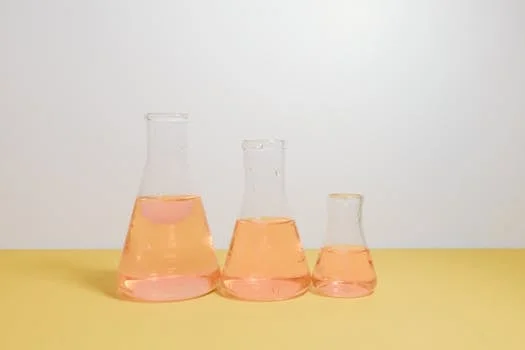
Etching processes, both wet and dry, generate wastewater streams characterized by high concentrations of dissolved metals such as copper (50–500 mg/L) and nickel (10–100 mg/L), alongside aggressive oxidants like hydrogen peroxide (1–10% in sulfuric peroxide mixtures, or SPM) and piranha acid (3:1 H₂SO₄:H₂O₂). Traditional wastewater treatment plants designed for municipal or light industrial use fail in semiconductor environments because standard precipitation and filtration cannot address the complex chemistry of these streams.
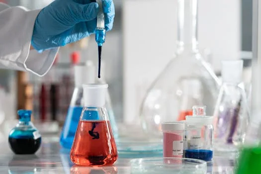
Specifically, the presence of organic acids, such as citric acid used in CMP wastewater treatment solutions, causes metal chelation, which prevents effective hydroxide precipitation. High residual peroxide concentrations interfere with traditional coagulation and flocculation by generating oxygen micro-bubbles that cause flocs to float rather than settle.
Fine colloidal silica, often smaller than 0.45 μm, easily bypasses standard sand filters, leading to downstream fouling of membranes and cooling towers. The regulatory stakes for failing to manage these complexities are high. A major semiconductor fabrication facility in Taiwan was fined $2.1M in 2023 for copper exceedances, where discharge levels reached 0.8 mg/L against a strict 0.5 mg/L limit, primarily due to the inadequate pretreatment of high-load etching streams.
To maintain compliance with EPA 40 CFR Part 469 and EU Directive 2010/75/EU, engineers must design systems that target specific contaminant thresholds. The following table outlines the primary regulatory limits that modern fab wastewater systems must achieve.
| Contaminant | EPA 40 CFR Part 469 Limit | EU Directive 2010/75/EU Limit | Typical Raw Etching Waste |
|---|---|---|---|
| Total Copper (Cu) | <0.5 mg/L | <0.5 mg/L | 50–500 mg/L |
| Total Fluoride (F) | <4.0 mg/L | <2.0 mg/L | 500–5,000 mg/L |
| Total Nickel (Ni) | N/A (varies by state) | <0.5 mg/L | 10–100 mg/L |
| Total Organic Carbon (TOC) | <100 mg/L | <50 mg/L | 500–2,000 mg/L |
| pH | 6.0–9.0 | 6.5–9.5 | 1.5–3.0 |
Contaminant Profile: What’s in Semiconductor Etching Wastewater?
Semiconductor etching wastewater contains dissolved metals, including copper (50–500 mg/L), nickel (10–100 mg/L), and aluminum (20–200 mg/L).Dissolved metals in etching wastewater, including copper (50–500 mg/L), nickel (10–100 mg/L), and aluminum (20–200 mg/L), fluctuate significantly based on whether the source is back-end-of-line (BEOL) etching or bulk wafer cleaning. These metals are often dissolved in strong mineral acids, including sulfuric acid (98% in SPM), hydrofluoric acid (0.5–5% in silicon etching), and nitric acid used for photoresist removal. The resulting pH typically ranges from 1.5 to 3.0, necessitating robust PLC-controlled chemical dosing for pH adjustment and peroxide quenching before any biological or membrane-based treatment can occur.
Oxidants represent a secondary but equally critical challenge. Hydrogen peroxide (H₂O₂) is ubiquitous in piranha and SPM cleaning steps, with concentrations reaching 30% in concentrated piranha baths. Residual ozone and persulfates from photoresist stripping add to the oxidative load, which can degrade RO membranes and ion-exchange resins if not neutralized. Organic loads are largely driven by tetramethylammonium hydroxide (TMAH), a common developer used at 1–5% concentrations, and photoresist residues that contribute to a Total Organic Carbon (TOC) profile of 500 to 2,000 mg/L. Finally, particulates such as colloidal silica and organic polymers from photoresist fragments require aggressive removal to prevent the physical plugging of high-efficiency treatment equipment.
| Waste Stream Component | Concentration Range | Primary Source | Treatment Challenge |
|---|---|---|---|
| Hydrogen Peroxide (H₂O₂) | 1% – 10% (SPM) | Wafer Cleaning / SPM | Membrane oxidation; inhibits settling |
| Dissolved Copper (Cu²⁺) | 50 – 500 mg/L | BEOL Etching / CMP | High toxicity; regulated at <0.5 mg/L |
| TMAH | 1,000 – 5,000 mg/L | Photolithography Developer | High nitrogen load; toxic to bio-sludge |
| Hydrofluoric Acid (HF) | 0.5% – 5% | Oxide Etching | Corrosive; fluoride discharge limits |
| Colloidal Silica | 100 – 1,000 mg/L | CMP Slurry / Etch Residue | Severe RO membrane scaling |
Treatment Technologies for Semiconductor Etching Wastewater: Process Flow and Efficiency Data
Electrochemical treatment systems for copper recovery operate at a current density of 10–50 A/m² to achieve 99% removal efficiency while producing high-purity metal byproduct. Unlike traditional precipitation, which creates hazardous copper hydroxide sludge, electrochemical cells capture copper as pure metal sheets on a cathode. For a typical 100 m³/h system, the CAPEX ranges from $1.2M to $2M, but the elimination of sludge disposal costs and the potential for metal resale provide a significant offset.
The treatment sequence begins with electrochemical copper recovery.These systems are typically positioned immediately after pH equalization to handle high-concentration metal streams before they are diluted by other fab effluents.
UV oxidation is the industry standard for breaking down high-concentration hydrogen peroxide and refractory organics. By utilizing 254 nm UV lamps in combination with controlled H₂O₂ or ozone dosing, systems can achieve TOC reduction rates of 70–90% and reduce peroxide to <1 mg/L. This process is energy-intensive, requiring 0.5–1.5 kWh/m³, but it is essential for protecting downstream industrial RO systems for semiconductor water reuse. For the final polishing stage, Membrane Capacitive Deionization (MCDI) is emerging as a preferred alternative to RO for low-TDS streams (<5,000 mg/L) due to its lower energy consumption (0.2–0.5 kWh/m³) and higher water recovery rates of up to 90%.
| Technology | Removal Efficiency | Energy Consumption | Typical CAPEX (100 m³/h) |
|---|---|---|---|
| Electrochemical Recovery | 99%+ (Copper/Nickel) | 1.5 – 3.0 kWh/kg metal | $1.2M – $2.0M |
| UV Oxidation (AOP) | 70–90% (TOC/H₂O₂) | 0.5 – 1.5 kWh/m³ | $0.8M – $1.5M |
| Reverse Osmosis (RO) | 98%+ (Total Ions) | 1.0 – 2.5 kWh/m³ | $1.5M – $2.5M |
| MCDI | 80–90% (TDS) | 0.2 – 0.5 kWh/m³ | $1.0M – $2.0M |
Designing a Semiconductor Etching Wastewater Treatment System: Step-by-Step Engineering Guide
Effective pretreatment requires a minimum equalization retention time of 2 to 4 hours.The first stage of design involves coarse screening (1–2 mm) to remove photoresist fragments, followed by a multi-stage pH adjustment tank. Using lime or caustic soda, the pH must be stabilized between 3.0 and 5.0 to optimize the kinetics of UV oxidation and electrochemical recovery. Instrumentation at this stage is critical; redundant online pH and ORP (Oxidation-Reduction Potential) meters must be integrated into the control loop to prevent "acid shocks" from reaching the membranes.
The core treatment train should follow a sequence of electrochemical copper recovery, UV oxidation, and membrane filtration. In the electrochemical stage, a current density of 20–50 A/m² is maintained to ensure the copper is plated effectively without excessive hydrogen evolution. Following metal recovery, the UV reactor applies a dose of 500–1,000 mJ/cm² to quench residual peroxides. Post-treatment involves pH neutralization to 7.0–8.0 and the use of a sludge dewatering for metal hydroxide precipitates for any residual solids generated during the neutralization of fluoride or silica.
Safety considerations are paramount in etching wastewater system design. Electrochemical cells generate small amounts of hydrogen gas, requiring localized exhaust ventilation and hydrogen monitoring. All piping and tankage for the etching stream must be constructed from acid-resistant materials, such as PVDF or Hastelloy, particularly in sections where hydrofluoric or piranha acids are present.
Cost Breakdown: CAPEX, OPEX, and ROI for Semiconductor Etching Wastewater Treatment
CAPEX for a 100 m³/h semiconductor wastewater treatment system incorporating RO and UV oxidation ranges from $2.3M to $4.0M in 2025 market valuations. This investment covers the primary equipment, high-alloy piping, automated control systems, and commissioning. While the initial cost is significant, the operational expenditures (OPEX) are increasingly manageable through technological advancements.
The ROI of an advanced etching wastewater system is driven by metal recovery, water reuse savings, and regulatory compliance.In a 200 m³/h fab environment, recovering 1 kg of copper per day can yield up to $20,000 annually in metal value. With industrial water costs ranging from $0.50 to $2.00 per cubic meter, a system achieving 90% recovery can save over $1M per year in raw water procurement and discharge fees.
| System Component | Estimated CAPEX (100 m³/h) | Annual OPEX (Power/Parts) | Primary ROI Driver |
|---|