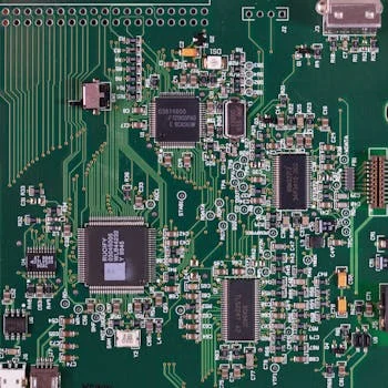
Chip Fab Wastewater Recycling: 2025 Engineering Specs, ZLD Costs & 95%+ Recovery Blueprint
A 10 MGD semiconductor fab consumes 3.65 billion gallons of water annually—equivalent to 50,000 households—driving fabs to adopt wastewater recycling systems achieving 95%+ recovery. Key contaminants like TDS (up to 2,500 mg/L), IPA (500–1,500 mg/L), and heavy metals (Cu, Ni, As) require hybrid treatment: MBR-RO for UPW reuse, FO-NF for ZLD, and MPPS for solvent recovery. CAPEX ranges from $2.5M for basic recycling to $40M for full ZLD, with OPEX at $0.36–$1.20/m³. This guide provides 2025 engineering specs, process flows, and cost data to design or evaluate fab-specific systems.Why Chip Fabs Must Recycle Wastewater: Water Demand, Contaminant Risks & CHIPS Act Mandates
A single semiconductor fabrication facility (fab) demands between 5 and 10 million gallons per day (MGD) of freshwater for wafer production, with new campuses often planning for multiple fabs, such as TSMC Arizona's projected 20 MGD total consumption (IEEE, 2022). This substantial water footprint, comparable to that of large municipalities, creates significant operational and environmental pressure. For instance, a 10 MGD fab consumes enough water to supply approximately 50,000 U.S. households annually, highlighting the urgent need for robust chip fab wastewater recycling solutions. Wastewater from semiconductor manufacturing is characterized by a complex contaminant profile that includes high concentrations of total dissolved solids (TDS) ranging from 500–2,500 mg/L, isopropyl alcohol (IPA) at 500–1,500 mg/L, and heavy metals such as copper (5–50 mg/L), nickel (2–20 mg/L), and arsenic (0.1–5 mg/L), alongside fluoride (10–100 mg/L) (EPA Semiconductor Effluent Guidelines, 2024). These contaminants necessitate advanced treatment to meet increasingly stringent discharge limits and enable water reuse. The CHIPS and Science Act of 2022 further amplifies this urgency, mandating a 30% reduction in freshwater use by 2027 and a 90% reduction by 2030 for incentivized projects (CHIPS Act Section 103(b)(2)(D)). Recycling efforts, while crucial, can paradoxically increase the concentration of TDS in the final effluent, making end-of-pipe zero-liquid-discharge (ZLD) systems essential to avoid permit violations and manage concentrate effectively (Carollo, 2024).| Fab Size (MGD) | Annual Water Consumption (Billion Gallons) | Equivalent Households Supplied Annually |
|---|---|---|
| 5 | 1.83 | 25,000 |
| 10 | 3.65 | 50,000 |
| 20 (Campus) | 7.30 | 100,000 |
Chip Fab Wastewater Streams: Sources, Contaminant Loads & Recycling Opportunities
| Process Step | Primary Contaminants | Typical Concentration Range (mg/L) | Recycling Opportunity |
|---|---|---|---|
| UPW Rinse | Low TDS, trace organics | TDS: <100, TOC: <5 | Activated carbon + Ion Exchange for UPW makeup |
| CMP Slurry | TSS, Silica, Copper | TSS: 500–2,000, SiO2: 100–500, Cu: 5–50 | Pretreatment for silica/metals, RO reject for non-critical uses |
| Etching | Fluoride, Acids (HF, HNO3) | F: 10–100, pH: 2–4 | Calcium precipitation for fluoride, neutralization |
| Photolithography | IPA, TMAH | IPA: 500–1,500, TMAH: 50–200 | MPPS for solvent recovery |
| RO Reject | High TDS, Salts | TDS: 2,000–5,000 | Cooling towers, scrubbers |
5 Proven Wastewater Recycling Technologies for Semiconductor Fabs: Removal Rates, Energy Use & CAPEX
Selecting the appropriate wastewater recycling technology for a semiconductor fab depends heavily on the specific contaminant profile, desired water quality for reuse, and budget constraints. Hybrid systems are typically required to achieve the high recovery rates and stringent purity levels demanded by chip manufacturing.- Membrane Bioreactor (MBR) + Reverse Osmosis (RO) for UPW Reuse: This integrated system is highly effective for treating mixed fab effluent to a quality suitable for reuse as makeup water for ultrapure water (UPW) systems. MBR systems for 99% TSS removal in semiconductor wastewater achieve over 99% removal of suspended solids and biological oxygen demand (BOD), while subsequent RO systems for 95% TDS removal in semiconductor water reuse can reduce total dissolved solids (TDS) by 95% or more. Energy consumption for this combination ranges from 1.5–2.5 kWh/m³. A 1 MGD system typically requires a CAPEX of $1.2M–$3M. A key limitation is the risk of silica fouling on RO membranes if not adequately pretreated.
- Forward Osmosis (FO) + Nanofiltration (NF) for ZLD Pre-Concentration: FO-NF offers a robust solution for pre-concentrating high-TDS streams before final ZLD, exhibiting lower fouling propensity compared to conventional RO. This technology achieves over 98% water recovery in the FO stage and 90% TDS removal in the NF stage, with energy use between 3–5 kWh/m³. CAPEX for a 1 MGD system is in the range of $2M–$5M. Its ability to handle challenging waste streams makes it ideal for achieving high water recovery rates (95%+) in ZLD applications.
- Macro Porous Polymer Sorption (MPPS) for Solvent Recovery: MPPS is a highly efficient and proven technology for recovering valuable organic solvents like isopropyl alcohol (IPA) from semiconductor wastewater. It achieves over 95% IPA removal and recovery, often with lower energy consumption than distillation or UF-RO (Veolia Water Technologies, 2023). Energy use is typically 0.8–1.2 kWh/m³. A 0.5 MGD MPPS system has an estimated CAPEX of $800K–$2M, providing significant operational savings through solvent reuse.
- Chemical Precipitation + Dissolved Air Flotation (DAF) for Heavy Metals & Fluoride: For streams with high concentrations of heavy metals (e.g., copper, nickel) and fluoride, chemical precipitation followed by clarification or DAF systems for TSS and FOG removal in chip fab wastewater is a proven method. This process can achieve over 99% removal of copper and nickel and 90% removal of fluoride. CAPEX for a 1 MGD system typically ranges from $500K–$1.5M. The primary limitation is the generation and subsequent disposal cost of chemical sludge, which can be $200–$500 per ton.
- Hybrid ZLD (FO-NF + Crystallizer): For fabs targeting ultimate water independence and zero discharge, a hybrid ZLD system combining FO-NF for bulk water recovery with a thermal crystallizer for final brine solidification is essential. This configuration achieves 99% water recovery and over 99.9% TDS removal. CAPEX for a 1 MGD system is higher, ranging from $5M–$10M, with OPEX at $1–$2/m³ due to the energy intensity of thermal processes. This approach is particularly relevant for high-TDS fabs, such as those found in Taiwan, facing strict discharge regulations.
| Technology | Contaminant Removal (%) | Energy Use (kWh/m³) | CAPEX ($/MGD) | OPEX ($/m³) | Scalability (MGD) |
|---|---|---|---|---|---|
| MBR + RO (UPW Reuse) | TSS >99%, TDS >95% | 1.5–2.5 | $1.2M–$3M | $0.40–$0.80 | 0.5–10+ |
| FO + NF (ZLD Pre-Conc.) | Water Rec. >98%, TDS >90% | 3–5 | $2M–$5M | $0.60–$1.00 | 0.5–5+ |
| MPPS (Solvent Recovery) | IPA >95% | 0.8–1.2 | $800K–$2M (for 0.5 MGD) | $0.30–$0.60 | 0.1–1+ |
| Chemical Precip. + DAF | Cu >99%, Ni >99%, F >90% | 0.2–0.5 | $500K–$1.5M | $0.20–$0.40 | 1–10+ |
| Hybrid ZLD (FO-NF + Crystallizer) | Water Rec. >99%, TDS >99.9% | 5–10 | $5M–$10M | $1.00–$2.00 | 0.5–5+ |
Designing a 95%+ Water Recovery System: Process Flow, Sizing & Contaminant-Specific Pretreatment
Cost Breakdown for Chip Fab Wastewater Recycling: CAPEX, OPEX & ROI for 1–10 MGD Systems
Evaluating the financial viability of chip fab wastewater recycling systems requires a detailed understanding of both capital expenditures (CAPEX) and operational expenditures (OPEX), alongside a clear return on investment (ROI) projection. These systems represent a significant investment, but offer substantial long-term savings and compliance benefits compared to traditional discharge methods. CAPEX for chip fab wastewater recycling systems varies widely based on capacity and desired recovery levels. A basic 1 MGD MBR-RO system for water reuse might have a CAPEX of $2.5M, whereas a comprehensive 10 MGD zero-liquid-discharge (ZLD) system, incorporating advanced FO-NF and crystallizer technologies, can reach up to $40M. A typical CAPEX breakdown includes equipment (60%), installation (20%), engineering (10%), and permits (10%). Operational expenditures (OPEX) for recycling systems generally range from $0.36–$1.20/m³, which is often competitive with or even lower than the cost of freshwater purchase combined with wastewater discharge fees, which can be $0.80–$2.50/m³. Discharge costs are particularly high for facilities with elevated TDS concentrations, as treatment plants may impose surcharges or prohibit discharge entirely (Carollo, 2024).| Technology/System Type | OPEX ($/m³) | Key OPEX Drivers |
|---|---|---|
| MBR-RO (Water Reuse) | $0.36–$0.80 | Energy, membrane cleaning/replacement, chemical dosing |
| FO-NF (Pre-Concentration) | $0.60–$1.00 | Energy, draw solution makeup, membrane cleaning |
| Hybrid ZLD (FO-NF + Crystallizer) | $1.00–$1.20+ | High energy for thermal crystallizer, brine disposal, chemical dosing |
| Chemical Precip. + DAF | $0.20–$0.40 | Chemicals, sludge disposal, energy for pumps |
Frequently Asked Questions: Chip Fab Wastewater Recycling Compliance, Scalability & Emerging Tech
Q: What are the 2025 discharge standards for semiconductor wastewater?
A: The U.S. EPA establishes stringent effluent limitations for semiconductor manufacturing. Key discharge standards include Total Suspended Solids (TSS) at 30 mg/L, Chemical Oxygen Demand (COD) at 120 mg/L, Copper (Cu) at 1.3 mg/L, Nickel (Ni) at 2.4 mg/L, Arsenic (As) at 0.1 mg/L, and Fluoride at 4 mg/L. Beyond these, the CHIPS Act mandates a 30% reduction in freshwater use by 2027 and 90% by 2030 for incentivized projects, pushing fabs towards near-zero discharge (Carollo, 2024).
Q: Can recycled water meet UPW standards for chip fabrication?
A: Yes, recycled water can meet ultrapure water (UPW) standards through advanced multi-stage treatment. Systems typically involve MBR-RO followed by polishing steps like activated carbon and ion exchange. Samsung Austin Semiconductor successfully recycles 60% of its UPW rinse water to meet UPW makeup requirements (UltraFacility, 2023). Achievable quality includes residual Total Organic Carbon (TOC) below 10 ppb and resistivity exceeding 18 MΩ·cm.
Q: What’s the energy cost of ZLD systems?
A: The energy cost for zero-liquid-discharge (ZLD) systems varies significantly by technology. Hybrid ZLD systems incorporating Forward Osmosis (FO) and Nanofiltration (NF) followed by a thermal crystallizer typically consume 3–5 kWh/m³. In comparison, MBR-RO systems for water reuse have lower energy demands, ranging from 1.5–2.5 kWh/m³. Thermal ZLD components are the primary drivers of higher energy consumption.
| Technology | Energy Use (kWh/m³) |
|---|---|
| MBR-RO (Water Reuse) | 1.5–2.5 |
| FO-NF (Pre-Concentration) | 3–5 |
| Hybrid ZLD (FO-NF + Crystallizer) | 5–10 |
Q: How do fabs handle PFAS in wastewater?
A: Per- and polyfluoroalkyl substances (PFAS) in wastewater are typically handled using granular activated carbon (GAC) or ion exchange (IX) resins, which can achieve over 90% removal. The EPA's 2024 final limits for PFOA and PFOS are set at 4 parts per trillion (ppt) in drinking water, impacting discharge requirements and necessitating effective removal strategies. Increasing TDS concentrations in recycled streams can also concentrate PFAS, requiring dedicated treatment (Carollo, 2024).
Q: What’s the lifespan of MBR/RO membranes in semiconductor wastewater?
A: The lifespan of membranes in semiconductor wastewater treatment varies with operating conditions and influent quality. MBR membranes (e.g., PVDF) typically last 5–7 years. RO membranes (e.g., polyamide) generally have a lifespan of 3–5 years. Membrane fouling, accelerated by high concentrations of silica (>100 mg/L) or IPA (>500 mg/L), and inadequate pretreatment, can significantly reduce membrane lifespan and increase operational costs.