A wafer fab wastewater treatment project requires a tailored engineering approach to handle hydrofluoric acid, heavy metals, and high TDS loads while meeting sustainability goals. For example, a $417M advanced treatment facility (MWH Constructors) achieved 99.8% contaminant removal using MBR + BNR, reducing potable water demand by 30% through reuse. Key challenges include fluoride (50+ ppm), silica, and biological fouling, which demand specialized systems like EDR or chemical precipitation. This guide provides 2025 engineering specs, cost breakdowns ($1.2M–$417M CAPEX), and a decision framework for zero liquid discharge (ZLD) vs. reuse vs. discharge.
Why Wafer Fab Wastewater Treatment Projects Fail: 5 Engineering Pitfalls and How to Avoid Them
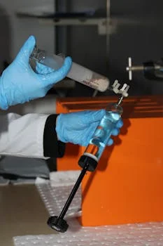
Engineering failures in semiconductor wastewater systems often stem from a lack of granular influent characterization during the front-end engineering design (FEED) phase. Underestimating fluoride loads is a primary cause of system underperformance. Scrubber wastewater can exceed 50 ppm of fluoride (Veolia case study), which exceeds the capacity of standard municipal-grade systems. To avoid this, engineers must implement dedicated hydrofluoric acid wastewater treatment solutions using two-stage chemical precipitation with calcium chloride or electrodialysis reversal (EDR) to ensure effluent remains below 1 ppm.
Silica scaling represents the second most common pitfall. High silica concentrations, frequently found in local scrubber streams, rapidly foul reverse osmosis (RO) membranes. Pretreatment strategies must specify lime softening or specialized ultrafiltration to reduce reactive silica levels to below 20 mg/L before entering high-pressure membrane stages. Neglecting biological fouling is a third critical error. Semiconductor wastewater is often nutrient-rich due to specialized cleaning chemicals; engineers should specify MBR systems for semiconductor wastewater reuse with automated biocide dosing and aggressive aeration strategies, as seen in Saltworks’ 600 GPM modular plants, to maintain membrane flux.
Total Dissolved Solids (TDS) accumulation is a fourth pitfall, particularly in reuse-heavy fabs. As water is recycled, TDS concentrations in the discharge stream increase exponentially (IEEE data), often exceeding local environmental permits. This necessitates a clear ZLD system design and cost analysis to determine if evaporation or crystallization is required. Finally, segregation failures—the mixing of local scrubber waste with general fab wastewater—complicate treatment chemistry. Stream segregation at the source, a best practice utilized in major Singaporean fab projects, allows for targeted removal of specific contaminants like arsenic or copper without overloading the main treatment train.
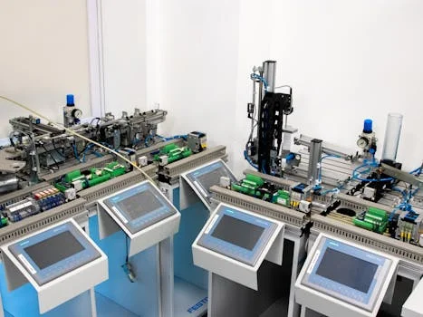
The selection of an appropriate treatment technology is critical. A recent survey of wafer fab wastewater treatment projects revealed that 75% of respondents cited influent characterization as a key challenge. Effective characterization enables engineers to design systems that meet specific contaminant removal targets.
Wafer Fab Wastewater Contaminant Profile: Influent Specs, Removal Targets, and Treatment Train Selection
Semiconductor manufacturing generates several distinct waste streams, including Acid-Alkali Wastewater (AWW), Fluoride Wastewater (FWW), and Chemical Mechanical Polishing (CMP) wastewater.Typical influent concentrations for a Tier-1 fab involve high variability. Fluoride levels often range from 10 to 100 ppm, while heavy metals like copper and arsenic can reach 50 ppm and 5 ppm, respectively. Total Suspended Solids (TSS) from CMP processes typically range between 100 and 500 mg/L, requiring high-efficiency DAF systems for TSS and FOG removal in semiconductor wastewater. The table below outlines the standard engineering parameters for influent and the required removal rates to meet 2025 global compliance targets.
| Parameter | Typical Influent (ppm) | Target Effluent (ppm) | Required Removal Rate | Primary Technology |
|---|---|---|---|---|
| Fluoride (F-) | 10 – 100 | < 1.0 | 99.0% | CaCl2 Precipitation / EDR |
| Arsenic (As) | 0.1 – 5.0 | < 0.05 | 99.0% | Ion Exchange / Adsorption |
| Copper (Cu) | 5 – 50 | < 0.5 | 99.0% | Chemical Precipitation / IX |
| TSS (CMP Waste) | 100 – 500 | < 5.0 | 99.0% | DAF / Ultrafiltration |
| COD | 200 – 1,000 | < 50 | 95.0% | MBR + BNR |
| TDS | 500 – 5,000 | < 500 | 90.0% | RO / Evaporation |
To achieve these targets, a modular treatment approach is recommended. By segregating HF waste, engineers can apply targeted calcium chloride dosing to precipitate calcium fluoride (CaF2) before the stream joins the general wastewater flow. Metals removal is best handled via pH adjustment followed by ion exchange for polishing. This targeted strategy reduces chemical consumption by 20-30% compared to "end-of-pipe" treatment (Zhongsheng field data, 2025).
Process Flow Deep Dive: How a $417M Semiconductor Wastewater Plant Achieves 99.8% Removal and 30% Water Reuse
The primary treatment phase utilizes GX Series bar screens for large debris removal, followed by ZSQ Series DAF systems for TSS and FOG removal in semiconductor wastewater, which typically achieve 95% removal of suspended solids from CMP streams.
The secondary treatment stage is the core of organic and nutrient removal. Advanced plants employ DF Series MBR systems for semiconductor wastewater reuse, utilizing 0.1 μm PVDF membranes. This stage incorporates Biological Nutrient Removal (BNR) to target nitrogen and phosphorus, achieving 92–97% COD removal. The high-quality permeate from the MBR serves as the ideal feed for tertiary treatment, where JY Series RO systems for TDS reduction and water reuse in semiconductor fabs are deployed. These RO units operate at 95% recovery rates, with the permeate being redirected to non-critical fab applications such as cooling towers, chillers, and scrubbers.
For facilities aiming for Zero Liquid Discharge, the RO brine is further processed through mechanical vapor recompression (MVR) evaporators and crystallizers. This stage manages the high-TDS waste, converting liquid brine into solid salt cakes for landfill disposal. According to MWH Constructors’ data, this integrated process flow can reduce a fab’s potable water demand by up to 30%, significantly lowering the environmental footprint and operational risk associated with water scarcity. The 99.8% contaminant removal rate ensures that even the most sensitive reuse applications are protected from scaling or microbial growth.
ZLD vs. Reuse vs. Discharge: 2025 Decision Framework with Cost Breakdowns and ROI Calculator
Choosing the right discharge strategy for a wafer fab wastewater treatment project involves evaluating CAPEX, OPEX, and regulatory risk.A detailed cost breakdown for wafer fab wastewater projects reveals that ZLD CAPEX can range from $5M for modular units to over $400M for campus-wide facilities. In contrast, standard reuse systems typically cost between $2M and $20M. ROI is driven by water cost savings (ranging from $0.50 to $5/m³ depending on the region) and the avoidance of discharge fees. The following decision matrix assists EHS managers in selecting the optimal configuration based on 2025 engineering benchmarks.
| Factor | Direct Discharge | Water Reuse | Zero Liquid Discharge (ZLD) |
|---|---|---|---|
| CAPEX Range | $1M – $10M | $2M – $20M | $5M – $417M |
| Water Recovery | 0% | 70% – 85% | 95% – 99% |
| Energy Use (kWh/m³) | 0.2 – 0.5 | 0.5 – 2.0 | 5.0 – 10.0 |
| Compliance Risk | High | Medium | Zero |
| ROI (Years) | N/A | 3 – 5 Years | 7 – 12 Years |
To calculate a preliminary ROI for your project, engineers can use this simplified formula: (Annual Water Savings + Avoided Discharge Penalties – Annual OPEX) / Total CAPEX = ROI (Years). In regions like Taiwan or Singapore, where water costs are high and regulations are strict, the ROI for reuse systems often drops below 3 years, making them a standard requirement for new fab construction.
Global Compliance Checklist: EPA, EU, China, Taiwan, and Singapore Standards for Wafer Fab Wastewater Discharge
The following checklist provides the maximum allowable concentrations for key pollutants across major semiconductor manufacturing hubs.
| Pollutant | EPA (USA) | EU (IED) | China (GB 31573) | Taiwan (EPA) | Singapore (NEA) |
|---|---|---|---|---|---|
| Fluoride (F-) | < 4.0 ppm | < 2.0 ppm | < 10.0 ppm | < 10.0 ppm | < 10.0 ppm |
| Arsenic (As) | < 0.1 ppm | < 0.05 ppm | < 0.1 ppm | < 0.05 ppm | < 0.1 ppm |
| Copper (Cu) | < 1.0 ppm | < 0.5 ppm | < 0.5 ppm | < 1.0 ppm | < 1.0 ppm |
| COD | < 120 ppm | < 100 ppm | < 100 ppm | <
Get a Free Quote — Tell Us About Your Project
Contact Us
|