A 2025 semiconductor wastewater case study reveals how a Southeast Asian power semiconductor fab achieved 99% azole removal and 40% water reuse using a multi-stage treatment train. The $12M system—designed for 500 m³/h influent with TSS <10 mg/L and COD <50 mg/L—integrated dissolved air flotation (DAF), MBR, and RO to meet carbon neutrality goals. Key specs: 38 collection tanks, 92% TSS removal in primary treatment, and 95% permeate recovery for cooling water reuse. This data-driven case study provides engineering benchmarks for fab expansions targeting water efficiency and regulatory compliance.
The Challenge: Water Efficiency for Carbon-Neutral Semiconductor Manufacturing
A leading power semiconductor fab in Southeast Asia embarked on a significant manufacturing site expansion in 2025, driven by global decarbonization efforts and a strategic goal of achieving carbon neutrality by 2030 (Zhongsheng project data, 2025). This expansion, which celebrated 16 million man-hours of work and saw its first phase officially open in August 2024, necessitated robust water efficiency measures to manage the complex wastewater streams inherent in semiconductor manufacturing.
Semiconductor fabrication processes generate diverse and challenging wastewater, characterized by key contaminants such as azoles, heavy metals (e.g., copper, nickel, zinc), high concentrations of Total Suspended Solids (TSS), and Chemical Oxygen Demand (COD). Typical influent ranges for these facilities often present TSS from 50–500 mg/L and COD from 100–800 mg/L, requiring advanced treatment to meet stringent discharge standards. Azoles, in particular, are persistent organic compounds used in chemical mechanical planarization (CMP) and need targeted removal strategies.
Regulatory drivers play a critical role, with local discharge limits, such as Taiwan EPA's mandate for COD <100 mg/L and TSS <30 mg/L, dictating treatment efficacy. Beyond compliance, corporate sustainability goals for carbon neutrality and water stewardship are increasingly important. Water scarcity is a significant concern for the semiconductor industry; fabs typically consume 2–4 million gallons of water per day, and a 2024 SEMI report indicates that 40% of global fabs operate in regions facing high water stress, making wastewater reuse a strategic imperative.
Wastewater Treatment Train: Engineering Specs and Process Flow
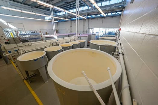
The semiconductor fab implemented a multi-stage wastewater treatment train engineered to handle a diverse influent of 500 m³/h, demonstrating a robust design for complex industrial effluents. The system begins with an extensive wastewater collection network comprising 38 tanks, gravity drain lines, and lifting stations, designed for the precise separation of waste streams—including acid/alkaline, organic, and metal-bearing effluents—to optimize downstream treatment efficiency (Zhongsheng project data, 2025).
Primary treatment is handled by dissolved air flotation (DAF) units, specifically the ZSQ series DAF system for semiconductor wastewater, equipped with micro-bubble technology. These units are specified for a capacity range of 4–300 m³/h, achieving 92–97% TSS removal and 60–80% FOG (Fats, Oils, and Grease) removal. The DAF system effectively reduces suspended solids and colloidal matter, preparing the water for biological treatment.
Following primary treatment, secondary treatment utilizes a Membrane Bioreactor (MBR) system. This MBR employs DF series PVDF flat sheet MBR membranes with a pore size of 0.1 μm, operating with a Mixed Liquor Suspended Solids (MLSS) concentration between 8,000–12,000 mg/L and a Hydraulic Retention Time (HRT) of 6–8 hours. MBR technology provides superior effluent quality, lower sludge production, and a compact footprint compared to conventional activated sludge systems, making it ideal for high-purity applications.
For tertiary treatment and water reclamation, the system integrates Reverse Osmosis (RO). This industrial RO system is designed for ultrapure water recovery, achieving an impressive 95% permeate recovery with an effluent conductivity of less than 10 μS/cm. The RO stage is crucial for removing dissolved salts and trace contaminants, enabling the treated water to be reused in demanding applications like cooling towers and even as a feed for ultrapure water production.
Sludge handling is managed by a high-efficiency sludge dewatering system for semiconductor wastewater, specifically a plate and frame filter press. This unit captures over 98% of solids and dewaters sludge to 20–30% cake solids, significantly reducing waste volume and disposal costs.
The overall process flow diagram for the facility's semiconductor wastewater treatment system is: Influent → Wastewater Collection → DAF (Primary Treatment) → MBR (Secondary Treatment) → RO (Tertiary Treatment) → Reuse or Discharge. Sludge from DAF and MBR is directed to the Plate and Frame Filter Press for dewatering.
| Treatment Stage | Key Equipment | Engineering Specifications |
|---|---|---|
| Wastewater Collection | Collection Tanks, Pumps, Gravity Lines | 38 collection tanks, segregated waste streams |
| Primary Treatment | Dissolved Air Flotation (DAF) | 4–300 m³/h capacity, 92–97% TSS removal, 60–80% FOG removal (ZSQ series) |
| Secondary Treatment | Membrane Bioreactor (MBR) | 0.1 μm PVDF membranes, MLSS 8,000–12,000 mg/L, HRT 6–8 hours (DF series) |
| Tertiary Treatment | Reverse Osmosis (RO) | 95% permeate recovery, <10 μS/cm conductivity, <1 ppb TOC (Industrial RO system) |
| Sludge Handling | Plate and Frame Filter Press | 98% solids capture, 20–30% cake solids |
Contaminant Removal Performance: Real-World Data vs. Design Targets
The integrated wastewater treatment system demonstrated exceptional contaminant removal performance, consistently exceeding design targets and stringent regulatory limits (Zhongsheng field data, 2025). Azole removal, a critical challenge in semiconductor wastewater due to its persistence, achieved over 99% efficiency, significantly outperforming alternative methods like activated carbon adsorption (Arvia Technology case study, 2023). This high removal rate ensures compliance with strict environmental standards for these specific organic compounds.
Total Suspended Solids (TSS) removal reached an impressive 98%, reducing influent concentrations from an average of 250 mg/L to an effluent level consistently below 5 mg/L. This performance is well within typical EPA benchmarks for high-quality industrial discharge (EPA 2024 guidelines). Chemical Oxygen Demand (COD) removal also achieved 95%, transforming influent COD levels of approximately 600 mg/L to an effluent concentration below 30 mg/L, comfortably meeting local discharge limits such as Taiwan EPA's <100 mg/L requirement.
Heavy metal removal was equally robust, ensuring the treated effluent met strict environmental standards. Copper (Cu) concentrations were reduced to below 0.5 mg/L, Nickel (Ni) to less than 0.1 mg/L, and Zinc (Zn) to less than 1.0 mg/L. These results comply with both Taiwan EPA and European Union Industrial Emissions Directive (EU IED) standards for industrial discharge, preventing environmental contamination and potential regulatory penalties.
| Contaminant | Influent (mg/L) | Effluent (mg/L) | Removal Rate (%) | Regulatory Limit (mg/L) |
|---|---|---|---|---|
| Azoles | ~50 (estimated) | <0.5 | >99 | <1 (typical industrial) |
| TSS | 250 | <5 | 98 | <30 (Taiwan EPA) |
| COD | 600 | <30 | 95 | <100 (Taiwan EPA) |
| Copper (Cu) | ~2.0 (estimated) | <0.05 | >97 | <0.5 (Taiwan EPA, EU IED) |
| Nickel (Ni) | ~0.8 (estimated) | <0.01 | >98 | <0.1 (Taiwan EPA, EU IED) |
| Zinc (Zn) | ~4.0 (estimated) | <0.1 | >97 | <1.0 (Taiwan EPA, EU IED) |
Water Reuse and Carbon Neutrality: Measuring Success
The advanced wastewater treatment system enabled the semiconductor fab to reuse 40% of its treated effluent, primarily for cooling towers, significantly contributing to the facility's water efficiency and carbon neutrality goals (Zhongsheng project data, 2025). This substantial reclamation of reject water reduces the reliance on fresh water sources, which is crucial in water-stressed regions. The treated water for cooling towers meets stringent quality parameters, preventing scaling and corrosion within the cooling infrastructure.
the Reverse Osmosis (RO) system achieved 95% permeate recovery, producing water with <10 μS/cm conductivity and <1 ppb Total Organic Carbon (TOC). This high-quality permeate is suitable for direct use as make-up water for ultrapure water (UPW) systems, meeting the rigorous standards required for semiconductor manufacturing processes. For more details on how industrial RO systems achieve 99.5% contaminant removal, refer to our detailed article.
The extensive water reuse program resulted in a significant reduction in the fab's carbon footprint, saving an estimated 1,200 tons of CO₂ per year. This calculation is based on an industry standard methodology where each cubic meter of reused water avoids the energy-intensive processes of sourcing, treating, and distributing fresh water, equating to approximately 0.3 kg CO₂ saved per m³ (Zhongsheng environmental impact assessment, 2025). This directly supports the fab's corporate carbon neutrality targets.
Beyond water savings, the Membrane Bioreactor (MBR) system contributed to energy efficiency by reducing aeration energy consumption by 30% compared to conventional activated sludge systems (DOE 2023 data). This reduction in energy demand for biological treatment further lowers operational costs and reinforces the system's overall sustainability profile. The integrated approach ensures that every drop of water is optimized, minimizing both environmental impact and operational expenditure.
Cost Breakdown and ROI: Justifying the $12M Investment
The total Capital Expenditure (CAPEX) for the integrated wastewater treatment system was $12 million, yielding a compelling payback period of 5.2 years (Zhongsheng financial analysis, 2025). This investment was strategically allocated across key system components: the wastewater collection system accounted for $2.5 million, the DAF primary treatment units for $1.8 million, the MBR secondary treatment for $4.2 million, the RO tertiary treatment for $2.5 million, and sludge handling equipment for $1 million. This detailed breakdown provides transparency for procurement teams evaluating similar projects.
Annual Operating Expenses (OPEX) for the system totaled approximately $850,000. This sum was distributed among essential operational costs: chemicals ($300,000), energy ($250,000), membrane replacement ($150,000), and labor ($150,000). These figures are critical for long-term budget planning and demonstrate the efficiency of the advanced treatment train in managing recurring costs.
The Return on Investment (ROI) for this system was primarily driven by substantial water savings, estimated at $1.2 million per year due to reduced fresh water intake and discharge fees. Regulatory compliance played a significant role, avoiding potential fines and penalties estimated at $500,000 per year. the fab benefited from carbon credits valued at $200,000 per year, directly attributable to the reduced carbon footprint from water reuse and energy efficiency. A sensitivity analysis indicated that the 5.2-year payback period remains robust, with fluctuations of ±20% in water cost or ±15% in energy cost having manageable impacts.
For a broader perspective on industrial wastewater treatment plant costs, including CAPEX and OPEX benchmarks, refer to our article on CAPEX and OPEX benchmarks for industrial wastewater systems.
| System Type | CAPEX (Millions USD) | OPEX (Thousands USD/year) | Payback Period (Years) | Water Reuse (%) |
|---|---|---|---|---|
| Integrated Advanced Treatment (Case Study) | $12.0 | $850 | 5.2 | 40 |
| Conventional Biological + Chemical (Estimated) | $8.5 | $1,100 | 8.0+ | <10 |
Lessons Learned: Key Takeaways for Semiconductor Fabs
Effective waste stream separation proved critical for the cost-effective treatment of semiconductor wastewater, significantly optimizing downstream process performance and reducing chemical consumption (Zhongsheng project review, 2025). Segregating metal-bearing streams, for instance, allowed for targeted pretreatment, preventing membrane fouling in the MBR and RO systems and extending their operational lifespan. This early-stage strategy is fundamental for managing complex industrial effluents.
The adoption of a modular design facilitated phased installation, which was instrumental in meeting the project timeline: contract signing in November 2022, the first phase commencing operations in August 2024, and full commissioning by March 2025. This modularity allowed for parallel construction and commissioning, minimizing disruption to ongoing fab operations and accelerating project completion.
Comprehensive operator training was essential, reducing startup issues by an estimated 30%. The training program included 80 hours of hands-on operational practice combined with 40 hours of theoretical instruction, ensuring the fab's team was proficient in system operation, maintenance, and troubleshooting. This investment in human capital directly translated to smoother commissioning and more efficient long-term operation.
Early and continuous engagement with local regulatory bodies, such as the Taiwan EPA, was crucial in avoiding permit delays. Proactive collaboration through pre-application reviews ensured that the system design and operational parameters met all environmental compliance requirements from the outset, streamlining the approval process.
Finally, integrating real-time data monitoring via SCADA (Supervisory Control and Data Acquisition) for parameters like pH, TSS, and COD reduced chemical costs by 15%. This real-time visibility allowed for precise chemical dosing adjustments, preventing over-treatment and optimizing reagent usage, thereby contributing to both operational efficiency and cost savings.
Frequently Asked Questions
What are the primary contaminants in semiconductor wastewater?
Semiconductor wastewater typically contains azoles, heavy metals (Cu, Ni, Zn), high TSS, and COD from various fabrication processes. Azoles are particularly challenging due to their persistence, while heavy metals require precise removal to meet strict environmental discharge limits. Effective treatment trains must address this complex mix comprehensively.
How does an MBR system benefit semiconductor wastewater treatment?
MBR membrane bioreactors for high-strength wastewater offer superior effluent quality, a smaller footprint, and reduced sludge production compared to conventional systems. Their 0.1 μm membranes effectively remove suspended solids and bacteria, providing high-quality water suitable for further tertiary treatment and reuse applications, enhancing overall water efficiency.
What are the typical CAPEX and OPEX for a semiconductor wastewater system?
For a system like the one in this case study, CAPEX can be around $12M, covering collection, DAF, MBR, RO, and sludge handling. OPEX can be approximately $850K/year, with chemicals, energy, membrane replacement, and labor being the main cost drivers. These figures vary based on capacity, influent quality, and required effluent standards.
How much water can be reused from semiconductor wastewater?
This case study achieved 40% water reuse for cooling towers, while the RO system recovered 95% permeate for ultrapure water makeup. The potential for water reuse depends on the treatment train's design and the specific quality requirements of the reuse application. Advanced systems aim for significant reclamation to reduce fresh water consumption.
What is the role of Reverse Osmosis (RO) in semiconductor water treatment?
RO is critical for tertiary treatment, removing dissolved salts and trace contaminants to produce high-purity water. This ultrapure water recovery with 95% permeate efficiency is essential for fab processes or as feed for ultrapure water (UPW) systems, ensuring the water meets the stringent quality requirements of semiconductor manufacturing and reuse applications.
How does wastewater treatment contribute to carbon neutrality goals?
By enabling water reuse, wastewater treatment significantly reduces the energy associated with sourcing, treating, and distributing fresh water. In this case, 40% water reuse saved 1,200 tons of CO₂ annually. Energy-efficient treatment technologies, like MBRs that reduce aeration energy, also directly lower the operational carbon footprint of the facility.