Semiconductor Wastewater Treatment Cost: 2025 Engineering Breakdown with CAPEX, OPEX & ROI Calculator
Semiconductor wastewater treatment costs vary widely based on system complexity and reuse goals. A 2025 benchmark shows CAPEX ranging from $5M for basic pretreatment to $417M for zero-liquid-discharge (ZLD) facilities (e.g., MWH Constructors’ $417M plant for a global fab). Operating costs average $0.91/m³ for reclaimed water, with payback periods of 3–7 years depending on water reuse rates and local utility costs. Key cost drivers include membrane replacement (30% of OPEX), chemical dosing, and energy for advanced oxidation processes.
Why Semiconductor Fabs Are Investing in Advanced Wastewater Treatment
Global semiconductor fabrication facilities typically consume 2–4 million gallons of water per day, per SEMI 2024 data, creating immense pressure to manage and reuse water effectively. This significant water footprint drives substantial investment in advanced wastewater treatment systems, primarily due to rising operational costs, stringent environmental regulations, and ambitious corporate sustainability targets.
Water scarcity and increasing utility charges directly impact a fab's bottom line, making water reuse a financial imperative. Simultaneously, regulatory bodies worldwide are tightening effluent discharge standards. The EU Industrial Emissions Directive 2010/75/EU, the U.S. EPA Effluent Guidelines for Semiconductors (40 CFR Part 469), and China’s GB 31573-2015 set strict limits on pollutants like heavy metals, fluorides, and organic compounds. Non-compliance can lead to severe penalties, often ranging from $10–$50/m³ of non-compliant discharge, varying by region and severity.
Beyond regulatory compliance, leading semiconductor manufacturers are setting aggressive sustainability goals. TSMC, for instance, aims for 30% water reuse by 2030, while Intel targets 100% water recycling in its Arizona fabs. These targets are driven by corporate social responsibility, brand reputation, and investor expectations. Investing in advanced wastewater treatment not only ensures compliance and reduces operational costs but also positions fabs as environmentally responsible leaders, mitigating risks and enhancing long-term resilience against water supply disruptions.
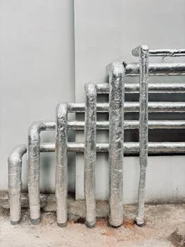
Semiconductor Wastewater Streams: Composition, Volume, and Treatment Challenges

Semiconductor fabrication generates diverse and complex wastewater streams, each presenting unique treatment challenges. Analysis of Top 5 market data indicates that acidic waste, primarily from etching processes involving hydrofluoric (HF) and nitric (HNO₃) acids, constitutes approximately 36% of total wastewater volume. Alkaline waste, often containing tetramethylammonium hydroxide (TMAH) from developing processes, accounts for 25%. Solvent waste, including isopropyl alcohol (IPA) and propylene glycol methyl ether acetate (PGMEA), makes up 15%, while heavy metals (such as copper and nickel) contribute 12%, and various mixed streams comprise the remaining 12%.
Key contaminants in these streams include fluorides at concentrations of 100–500 mg/L, total suspended solids (TSS) ranging from 50–200 mg/L, chemical oxygen demand (COD) between 200–1,000 mg/L, and trace metals like arsenic (As) and antimony (Sb). For a mid-sized fab producing 20,000–30,000 wafers/month, typical wastewater flow rates can range from 500–5,000 m³/day. These waste streams present significant treatment challenges due to extreme pH swings (often from 1 to 12), high salinity (5,000–10,000 mg/L TDS), and variable organic loads, requiring robust and adaptable treatment solutions.
| Wastewater Stream Type | Typical Volume % | Key Contaminants | Concentration Range |
|---|---|---|---|
| Acidic Waste (HF, HNO₃) | 36% | Fluorides, Acids, Metals | 100-500 mg/L (Fluoride) |
| Alkaline Waste (TMAH) | 25% | Alkaline compounds, Organics | pH 10-12 |
| Solvent Waste (IPA, PGMEA) | 15% | Organic Solvents, COD | 200-1,000 mg/L (COD) |
| Heavy Metals (Cu, Ni) | 12% | Copper, Nickel, Arsenic | Trace to 50 mg/L |
| Mixed Streams | 12% | Various, High TSS | 50-200 mg/L (TSS) |
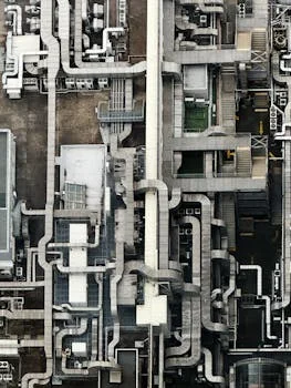
Treatment Technologies Compared: CAPEX, OPEX, and Performance for Semiconductor Wastewater
Selecting the optimal wastewater treatment technology for a semiconductor fab involves a careful balance of capital expenditure (CAPEX), operational expenditure (OPEX), and desired performance outcomes. Each technology offers distinct advantages and trade-offs tailored to specific contaminant profiles and reuse goals.
Chemical treatment, often used for initial pH adjustment and heavy metal removal, typically involves coagulation, flocculation, and precipitation. It has a CAPEX of $2M–$10M and OPEX ranging from $0.50–$1.20/m³, achieving approximately 90% TSS removal and 80% heavy metal removal (per Top 5 data). Its strength lies in cost-effective pretreatment for bulk contaminants.
Biological treatment, including conventional activated sludge, Biological Nutrient Removal (BNR), and MBR systems for semiconductor wastewater reuse, effectively removes organic matter and nitrogen. MBR systems, known for their compact footprint and high effluent quality, have a CAPEX of $5M–$20M and OPEX of $0.80–$1.50/m³. They can achieve 95% COD removal and 99% TSS removal, as demonstrated in a Top 1 case study. To understand how MBR membrane modules work for semiconductor wastewater, further technical details are available.
Membrane filtration, such as RO systems for ultra-pure water recovery in fabs and nanofiltration (NF), is crucial for removing dissolved solids, salts, and specific ions like fluoride. RO/NF systems have a CAPEX of $3M–$15M and OPEX of $1.00–$2.00/m³. They excel in achieving 99% TDS removal and 95% fluoride removal, producing water suitable for various reuse applications. For insights into RO system design for high-salinity semiconductor wastewater, explore our detailed article.
Advanced oxidation processes (AOPs), including UV/H₂O₂ or ozone, are employed for recalcitrant organic compound destruction and pathogen inactivation. AOPs have a CAPEX of $1M–$8M and higher OPEX of $1.50–$3.00/m³ due to energy and chemical consumption, but they can achieve 90% organic removal and 99% pathogen kill.
Finally, Zero-Liquid-Discharge (ZLD) systems integrate multiple technologies (e.g., MBR, RO, evaporators, crystallizers) to maximize water recovery and eliminate liquid waste discharge. ZLD represents the highest investment, with CAPEX ranging from $50M–$417M and OPEX from $2.00–$5.00/m³, but it achieves 100% water recovery, as seen in the Top 1 $417M plant example.
| Technology | Typical CAPEX (M$) | Typical OPEX ($/m³) | Key Performance |
|---|---|---|---|
| Chemical Treatment | $2 - $10 | $0.50 - $1.20 | 90% TSS, 80% Heavy Metal Removal |
| Biological Treatment (BNR/MBR) | $5 - $20 | $0.80 - $1.50 | 95% COD, 99% TSS Removal |
| Membrane Filtration (RO/NF) | $3 - $15 | $1.00 - $2.00 | 99% TDS, 95% Fluoride Removal |
| Advanced Oxidation (UV/H₂O₂) | $1 - $8 | $1.50 - $3.00 | 90% Organic Removal, 99% Pathogen Kill |
| Zero-Liquid-Discharge (ZLD) | $50 - $417 | $2.00 - $5.00 | 100% Water Recovery |
Cost Breakdown: CAPEX and OPEX for Semiconductor Wastewater Treatment Systems
A granular understanding of CAPEX and OPEX components is essential for accurate budgeting and identifying cost-saving opportunities in semiconductor wastewater treatment. For large-scale projects, such as the $417M ZLD plant referenced, equipment costs typically account for 40% of the total CAPEX, encompassing membranes, pumps, reactors, and instrumentation. Civil and structural works, including tanks, buildings, and foundations, represent another 30%. Engineering, design, and project management services contribute 20%, while permitting, regulatory compliance, and contingency make up the remaining 10%.
Operating expenditure (OPEX) is dominated by energy consumption, which accounts for approximately 30% due to the power required for pumps, aeration in biological systems, and high-pressure pumps in RO. MBR systems typically consume 0.8–1.2 kWh/m³, while RO systems, particularly for high-salinity streams, require 1.5–2.5 kWh/m³ (per DOE 2024 benchmarks). Membrane replacement is another significant OPEX component, contributing 25%. PVDF MBR membranes generally last 5–8 years with replacement costs ranging from $50–$100/m², while RO membranes have a shorter lifespan of 3–5 years and cost $30–$60/m² to replace. For more details on MBR membrane modules, refer to our product page.
Chemical costs represent about 20% of OPEX, with coagulants and flocculants for pretreatment costing $0.10–$0.30/m³ and pH adjustment chemicals (acids/bases) costing $0.20–$0.50/m³. Precision chemical dosing for pH control and heavy metal removal is crucial for efficient operation. Labor for operation and maintenance constitutes 15% of OPEX, and routine maintenance, spare parts, and unforeseen repairs account for the final 10%.
| Cost Category | CAPEX Breakdown (Typical %) | OPEX Breakdown (Typical %) |
|---|---|---|
| Equipment (Membranes, Pumps, Reactors) | 40% | - |
| Civil/Structural (Tanks, Buildings) | 30% | - |
| Engineering & Design | 20% | - |
| Permitting & Contingency | 10% | - |
| Energy (Pumps, Aeration, RO) | - | 30% (0.8-2.5 kWh/m³) |
| Membrane Replacement | - | 25% ($30-$100/m² every 3-8 years) |
| Chemicals (Coagulants, pH adjustment) | - | 20% ($0.30-$0.80/m³) |
| Labor (Operations & Maintenance) | - | 15% |
| Maintenance & Spare Parts | - | 10% |
Water Reuse ROI: How to Calculate Payback for Your Fab’s Wastewater Treatment Investment
Calculating the Return on Investment (ROI) for advanced semiconductor wastewater treatment is critical for justifying significant capital outlays to stakeholders. The payback period, a key metric, can be determined using the formula: Payback Period = (CAPEX - Incentives) / (Annual Savings - Annual OPEX). This calculation quantifies the time it takes for the initial investment to be recouped through operational savings and avoided costs.
Annual savings are derived primarily from two sources: the value of reclaimed water and avoided regulatory penalties. Reclaimed water for industrial use can save an average of $0.91/m³ compared to purchasing fresh potable water (per Top 2 data), while avoiding penalties for non-compliance can translate to savings of $10–$50/m³ of wastewater, depending on local regulations. various incentives can significantly reduce the net CAPEX. The U.S. Inflation Reduction Act (IRA) of 2022 offers up to 30% tax credits for water reuse projects, and programs like EU Horizon Europe grants or regional rebates (e.g., Singapore’s Water Efficiency Fund) provide additional financial support.
Consider an example calculation: a fab invests $10M in CAPEX for an advanced water reuse system. With annual OPEX of $1.5M and annual savings from reduced water purchases and avoided penalties totaling $3M, the payback period would be (assuming no incentives for simplicity) ($10M - $0) / ($3M - $1.5M) = 6.67 years. If there were, for example, $2M in incentives, the payback would drop to ($10M - $2M) / ($3M - $1.5M) = 5.33 years. Sensitivity analysis reveals how payback periods fluctuate with key variables; increasing the water reuse rate from 50% to 90% or operating in regions with higher local utility costs (e.g., $2.00/m³ vs. $0.50/m³) can dramatically shorten the payback period, making the investment more attractive. This framework allows fab managers to evaluate the financial viability under various operational and market conditions.
| Metric | Value | Notes |
|---|---|---|
| Example CAPEX | $10,000,000 | Initial investment cost |
| Example Annual OPEX | $1,500,000 | Operational costs per year |
| Example Annual Savings (Water Reuse) | $3,000,000 | Based on $0.91/m³ reclaimed water + avoided penalties |
| Potential Incentives | Up to 30% of CAPEX | U.S. IRA, EU Horizon Europe, regional grants |
| Calculated Payback Period (No Incentives) | 6.67 years | ($10M - $0) / ($3M - $1.5M) |
| Calculated Payback Period (with $2M Incentives) | 5.33 years | ($10M - $2M) / ($3M - $1.5M) |
Case Study: $417M ZLD Facility for a Global Semiconductor Manufacturer
A confidential global semiconductor manufacturer invested $417M in a Zero-Liquid-Discharge (ZLD) facility, demonstrating the significant commitment required for comprehensive wastewater treatment and reuse. This project, detailed by MWH Constructors, was designed to treat 5,000 m³/day of diverse fab wastewater, achieving an ambitious 90% water reuse rate, with the remaining 10% processed to ZLD.
The sophisticated treatment train deployed included Biological Nutrient Removal (BNR) and Membrane Bioreactor (MBR) for initial organic and nutrient removal, followed by Reverse Osmosis (RO) for dissolved solids and salt separation. Advanced Oxidation Processes (AOPs) were then used to break down recalcitrant organics, with the final reject stream directed to an evaporator/crystallizer system to achieve ZLD. This multi-stage approach ensured maximum contaminant removal and water recovery.
The facility achieved exceptional performance, demonstrating 99.9% TSS removal, 99.5% fluoride removal, and overall 100% water recovery from the initial wastewater stream. The economic benefits were substantial, with estimated annual savings of $12M from avoided potable water purchases and an additional $2M/year from avoided regulatory penalties. Key lessons learned from this large-scale endeavor included the critical importance of extensive pilot testing for high-salinity streams to optimize membrane performance and fouling control. implementing a modular design approach was found to reduce CAPEX by an estimated 15% by allowing for phased construction and future expansion flexibility.
Frequently Asked Questions
The average cost per cubic meter for semiconductor wastewater treatment is approximately $0.91/m³ for reclaimed water, though this can vary significantly. Key cost drivers include energy consumption for pumps and aeration (0.8–2.5 kWh/m³), membrane replacement ($30–$100/m² every 3–8 years), and chemical dosing for pH adjustment and contaminant removal ($0.30–$0.80/m³).
Building a semiconductor wastewater treatment plant typically takes 12–24 months for design and construction, with an additional 6–12 months required for permitting and regulatory approvals, as seen in the timeline for large-scale projects like the $417M ZLD facility.
For acidic waste treatment, chemical precipitation ($0.50–$1.20/m³) is often the most cost-effective initial step for bulk neutralization and heavy metal removal. However, for higher purity requirements or water reuse, membrane filtration ($1.00–$2.00/m³) may be necessary to remove dissolved solids and specific ions.
Yes, semiconductor wastewater can be treated to drinking water standards, but this typically incurs 2–3 times the cost of treating it for industrial reuse, primarily due to the additional advanced purification steps and stringent monitoring required, as outlined by EPA 2024 guidelines.
Several incentives are available for water reuse projects. In the U.S., the Inflation Reduction Act of 2022 offers up to 30% tax credits. The EU provides grants through programs like Horizon Europe, and various regional governments, such as Singapore with its Water Efficiency Fund, offer specific rebates and subsidies to encourage sustainable water management.