For 2026 procurement, semiconductor UPW system SEMI F63 compliance means matching point-of-distribution water quality to the fab node and proving control at point of use. The baseline retains ≥18.2 MΩ·cm resistivity, TOC <1 μg/L, and a $2.5–5 million CapEx range for a 50 m³/h plant.
Semiconductor UPW system SEMI F63 compliance 2026: what must be verified?
Semiconductor UPW compliance in 2026 is confirmed at the point of distribution, not inferred from a nameplate. ASTM D5127-13 Type E-1.3 lists 18.2 MΩ·cm at 25°C and 1 μg/L TOC, while SEMI F63-1224 is a technical guide for setting facility criteria. Use node targets, monitoring, and failover tests together.
The standards terminology needs precision before procurement. The ASTM page identifies the document as ASTM D5127-13, and E-1.3 as one water classification rather than a separate standard called ASTM E-1.3. ASTM’s published table ties Type E-1.3 to a 0.065–0.032 micron linewidth range and applies its recommendations at the point of distribution. Earlier article language used ASTM E-1.3 as a shorthand; the corrected designation is ASTM D5127-13 Type E-1.3.
SEMI’s current product listing identifies SEMI F63-1224 as the current revision. The listing describes F63 as technical information and suggested guidelines, not a regulation that automatically mandates one universal water quality. It covers new or retrofit facilities with line widths of 32 nm and smaller and should be used with SEMI F61 and SEMI F75. The dedicated semi f63 article can carry the standard-specific discussion, while this page stays focused on system compliance, cost, and troubleshooting.
SEMI’s standards FAQ assigns different jobs to the guides: F61 establishes typical UPW system definitions, F63 supports equipment criteria and operating parameters, and F75 supports quality monitoring through point of use. A fab specification should therefore state which edition, sampling location, analytical method, alarm limit, and release criterion apply. Do not treat a supplier’s generic 18.2 MΩ·cm claim as evidence that every contaminant is controlled.
Why do sub-7nm fabs lose yield when UPW resistivity falls below 18.2 MΩ·cm?
Sub-7nm fabs lose process margin when UPW resistivity falls below 18.2 MΩ·cm because ionic contamination can reach wet-processing steps and disturb wafer surfaces. The resistivity alarm is a symptom, not a complete diagnosis. A stable reading must be confirmed with temperature compensation, TOC, particles, silica, dissolved oxygen, and trend data.
Smaller transistors and denser circuitry place strict limits on ultrapure water. Trace contaminants can cascade into defects and yield loss. The original production estimate states that water-related contaminants account for 8–12% of wafer defects in sub-7nm processes; treat that figure as a site-specific planning claim unless the fab has its own defect correlation study. In the same supplied case, a 5nm fab cut yield losses by 18% after raising UPW resistivity from 17.8 MΩ·cm to 18.2 MΩ·cm.
Particles, dissolved organics, and ions can appear as gate oxide failures, metal corrosion, or poor photoresist adhesion. A single 300mm wafer at the 5nm node can cost upwards of $10,000, so a 1% yield loss can exceed $1 million in lost revenue per month for a mid-sized fab. Those figures are business-model inputs, not universal prices. Finance teams should replace them with actual wafer value, cycle time, and defect attribution.
Most plants we size for run near the lower end of the alarm envelope, then need short-term recovery capacity during maintenance or tool additions. That makes a trend-based control plan more useful than a single pass/fail sample. Set action limits before the first excursion, and record whether the sample came from the tank, loop return, or point of use.
What UPW limits do ASTM D5127 Type E-1.3 and SEMI F63 require in 2026?
ASTM D5127 Type E-1.3 recommends 18.2 MΩ·cm resistivity at 25°C, 1 μg/L TOC, 10 μg/L on-line dissolved oxygen, and 0.5 μg/L dissolved silica in its published table. SEMI F63-1224 provides technical guidance for semiconductor UPW criteria, but the fetched SEMI page does not support calling every value a legal mandate. Final limits must be approved by the fab process owner and tied to its metrology capability.
The same ASTM table lists 500 particles/L above 0.05 μm for Type E-1.3, with separate particle bands and sampling conventions. That value is not equivalent to the planning table below, which uses particles per mL and node-specific internal targets. Keep both contexts visible. A procurement document should specify the unit, particle-size threshold, sample volume, instrument, and whether the limit is an average, maximum, or excursion trigger.
The original draft described a 2026 SEMI F63 revision and said that F63 mandates limits for advanced nodes. The current SEMI listing instead shows F63-1224 as the current revision and calls the document a guide. It is more defensible to say that the fab adopts F63-1224-informed criteria. Taiwan’s SEMI S2/S8 requirements and EU REACH implications also require separate legal and facility review; they should not be presented as universal UPW chemistry limits without a project jurisdiction and resin specification.
Specs may tighten by node. The supplied design envelope uses TOC <1 μg/L for 7nm and TOC below 0.5 μg/L for 3nm. Treat those values as project targets to validate with the process integration team, not as a claim that one public standard assigns every node the same limit. Verify the train against node-specific limits before release to production.
The following table preserves the supplied node-planning values. It is a design comparison, not a transcription of every value in ASTM D5127 or SEMI F63-1224:
| Parameter | 3nm Node | 5nm Node | 7nm Node | 14nm+ Node |
|---|---|---|---|---|
| Resistivity (MΩ·cm) | >18.2 | >18.2 | >18.2 | >18.0 |
| TOC (μg/L) | <0.5 | <0.75 | <1.0 | <1.0 |
| Particles (>0.05 μm/mL) | <0.1 | <0.5 | <1.0 | <1.0 |
| Dissolved Silica (ppb) | <0.2 | <0.2 | <0.2 | <0.5 |
| Colloidal Silica (ppb) | <0.3 | <0.3 | <0.3 | <1.0 |
| Dissolved Oxygen (ppb) | <5 | <8 | <10 | <10 |
| Bacteria (CFU/mL) | <0.1 | <0.1 | <0.1 | <0.1 |
For initial-stage purification, semiconductor-grade RO remains the main barrier for dissolved ions and many organics. The original equipment pathway is retained here: Learn more about semiconductor-grade RO systems for UPW pre-treatment. A complete specification should also state feed conductivity, recovery, rejection, SDI, temperature, and the allowable permeate trend before EDI.
Feed solids still affect downstream reliability. Where a project has suspended-solids or colloidal carryover, a High-Efficiency Sedimentation Tank (Lamella Clarifier) may be evaluated upstream of filtration, but its use must be justified by raw-water testing. It is not a substitute for semiconductor-grade polishing or final particle control.
Which purification stages belong in a semiconductor UPW train?
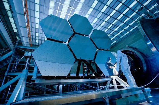
Semiconductor UPW trains use separate unit operations because ions, organics, dissolved gases, particles, and microorganisms fail in different ways. The SEMI F63 listing notes that the design and configuration of a typical UPW system, with its elements and unit processes, is described in SEMI F61. That split supports the practical distinction between a membrane makeup loop and a polishing loop using ion exchange and UV oxidation, although each fab must validate the exact chemistry and recovery arrangement.
Reverse osmosis removes over 99% of dissolved ions and a large share of organics in the supplied design basis. Feed water should hold a Silt Density Index below 3, typically through multimedia filtration and cartridge filters. The RO stage should be trended by normalized flow, differential pressure, conductivity rejection, and temperature. One weak pre-treatment step can shorten membrane life and push ionic load into EDI.
Electrodeionization then reaches 18.2 MΩ·cm resistivity without chemical regenerants when feed conductivity is already below 10 μS/cm. EDI needs stable feed chemistry and adequate hydraulics. UV oxidation with 185nm and 254nm lamps breaks residual TOC toward sub-μg/L levels. Lamp intensity, sleeve condition, dose, and replacement hours belong in the operating record.
Sub-micron filtration at 0.05 μm pore size provides the final particle barrier; manage fouling with adequate cross-flow and a defined integrity test. Polishing loops recirculate UPW through purification media during low demand or downtime to hold resistivity. A typical flow is raw water → pre-treatment → RO → EDI → UV oxidation → sub-micron filtration → polishing loop → point-of-use.
Implementing precise chemical dosing for UPW pre-treatment is vital for protecting downstream purification stages. Explore solutions for precise chemical dosing in UPW pre-treatment. Dose control should be locked to raw-water alkalinity, oxidant demand, membrane compatibility, and the project’s discharge constraints.
For maintaining system integrity and preventing microbial growth within UPW loops, on-site ClO₂ generation offers one sanitization option. Discover the benefits of on-site ClO₂ generation for UPW loop sanitization. The sanitation method must be compatible with wetted materials, validated for residual removal, and followed by a documented rinse-up before production release.
Advanced TOC removal, crucial for sub-7nm nodes, can be further assessed through resin and adsorption controls. Learn about advanced TOC removal for semiconductor UPW. Avoid assuming that a low TOC result at the tank proves the same result at the farthest point of use.
How should a fab size UPW capacity and design N+1 redundancy?
Fab UPW capacity is commonly estimated as wafer area processed per day multiplied by 4.5–7 liters per cm². A fab processing 100,000 cm² daily therefore needs 450–700 m³ of UPW per day. This estimate is a starting point, not a final balance. Add rinse recipes, tool population, peak demand, recovery losses, reject flows, planned maintenance, and future node expansion.
SEMI F63 is used by facility teams to set quality expectations, while redundancy is a project design decision that must be written into the user requirement specification. The supplied basis calls for N+1 coverage on critical RO trains, EDI, and UV sterilizers. Define the failed-train capacity, automatic isolation, restart sequence, buffer volume, and alarm handoff. Test failover before commissioning, at peak and low demand.
At point of use, deliver 18.2 MΩ·cm resistivity with POU polishers and recirculation loops using PVDF piping and zero-dead-leg valves to limit stagnation. A 7nm fab in Taiwan reported a 30% reduction in operational downtime after adding a redundant EDI skid; use that supplied case as a hypothesis to test against the site’s own downtime ledger. N+1 is not proven until the remaining trains carry the required flow and quality during a controlled failure.
The following table illustrates typical UPW system capacities and their associated daily demand ranges, aiding in the initial sizing process:
| System Capacity (m³/h) | Daily Demand Range (m³/day) | Typical Fab Node |
|---|---|---|
| 20 | 480 - 700 | 14nm - 28nm |
| 50 | 1200 - 1750 | 7nm - 10nm |
| 100 | 2400 - 3500 | 5nm - 7nm |
| 200 | 4800 - 7000 | 3nm - 5nm |
Use the table to screen options, then complete a 24-hour mass balance. A 50 m³/h skid does not necessarily deliver 1200 m³/day of usable UPW if recovery, cleaning, or polishing-loop constraints reduce availability. Procurement should request contracted net production, quality at the farthest POU, and performance during one train out of service.
What CapEx and OpEx should a 50–200 m³/h UPW system budget?
For 2026, CapEx for a typical 50 m³/h UPW system is estimated at $2.5 million to $5 million, and $5 million to $10 million for a 200 m³/h system. These are budgetary ranges, not quotations. Site class, cleanroom interfaces, utility tie-ins, materials, automation, validation, freight, and local labor can move the total substantially.
Cost share is roughly RO 30%, EDI 25%, UV 15%, and piping/instrumentation/controls/installation 30%. OpEx generally falls between $0.50 to $1.20 per 1,000 gallons, with energy about 40%, chemicals 20%, maintenance and spares 25%, and labor 15%. ROI is driven by yield and availability: a fab that prevents $3 million in annual yield losses can recover CapEx in 18–24 months under the supplied model.
Also budget annual compliance audits ($50,000 to $100,000), critical spare parts, operator training, laboratory services, calibration, membrane cleaning, resin replacement, and validation water. Procurement teams comparing costs should separate one-time construction from recurring consumables. The Semiconductor UPW System Cost: 2026 CAPEX, OPEX & ROI Breakdown for Fabs provides a sibling cost view; use one consistent boundary when comparing both models.
The following table provides a generalized cost breakdown for semiconductor UPW systems, aiding in budgetary planning:
| Cost Category | Estimated Percentage of Total CapEx | Estimated OpEx per 1,000 Gallons |
|---|---|---|
| Reverse Osmosis (RO) | 30% | $0.15 - $0.30 |
| Electrodeionization (EDI) | 25% | $0.10 - $0.25 |
| UV Sterilization | 15% | $0.05 - $0.10 |
| Piping, Instrumentation & Controls | 30% | $0.20 - $0.40 |
| Total Estimated CapEx | Full | |
| Total Estimated OpEx | $0.50 - $1.20 |
Check the arithmetic boundary in the table before approval. The category percentages sum to the full CapEx, while the component OpEx ranges are budget allocations that may overlap with site services or operator labor. A lifecycle model should show annual volume, reject water, electricity tariff, chemical unit price, replacement intervals, downtime cost, and the cost of an emergency bypass.
Semiconductor UPW resistivity drop troubleshooting EDI RO
Semiconductor UPW resistivity drop troubleshooting EDI RO starts by confirming the measurement before opening equipment. Compare the online reading with a calibrated grab sample, verify temperature compensation, and check whether the excursion appears at the tank, loop return, or POU. Then separate EDI performance, RO rejection, sensor drift, and contamination introduced after polishing.
A resistivity drop below 18.0 MΩ·cm usually points to EDI issues, RO membrane fouling, ion breakthrough, or a measurement problem. Verify EDI voltage and flow, inspect and clean RO membranes, confirm pre-treatment performance, and compare conductivity before and after each barrier. A TOC spike above 2 μg/L often follows UV lamp failure, organic breakthrough on RO, or biofilm in the polishing loop.
Replace UV lamps when output is outside the validated dose, sanitize the loop when the approved method allows it, and track RO rejection. Particle counts above 1 particle/mL can come from filter failure, piping leaks, pump cavitation, or sampling contamination. Replace filters only after an integrity check where practical. Inspect piping, check pump seals, and review the sample port before declaring a process failure.
Use a fixed troubleshooting matrix so diagnosis stays consistent under production pressure. The first response should protect wafers and preserve samples; the second should isolate the failed barrier; the third should prove recovery through repeated samples at defined locations. Review trends back to the last cleaning, sanitation, membrane change, and calibration event.
The following matrix provides a guide for diagnosing and resolving common UPW system issues:
| Symptom | Likely Cause | Diagnostic Steps | Recommended Fix |
|---|---|---|---|
| Resistivity Drop (<18.0 MΩ·cm) | EDI Failure / RO Membrane Fouling / Ion Breakthrough | Verify EDI voltage; Inspect/clean RO membranes; Check pre-treatment SDI/turbidity. | Repair/replace EDI module; Clean RO membranes; Optimize pre-treatment. |
| TOC Spike (>2 μg/L) | UV Lamp Failure / Organic Breakthrough / Biofilm | Check UV lamp output/hours; Monitor RO rejection rate; Inspect polishing loop for growth. | Replace UV lamps; Sanitize loop (e.g., ozone); Troubleshoot RO performance; Implement enhanced sanitization protocol. |
| Particle Count Excursion (>1/mL) | Filter Failure / Piping Leak / Pump Cavitation | Perform integrity test on filters; Visually inspect piping and connections; Check pump operation and seals. | Replace affected filters; Repair/replace piping; Service or replace pump. |
| High Feed Water SDI | Ineffective Pre-treatment / Filter Clogging | Inspect multimedia filters; Check cartridge filter condition; Analyze raw water quality. | Backwash/replace multimedia filters; Replace cartridge filters; Adjust pre-treatment dosing/filtration. |
For critical applications requiring on-site disinfection to prevent microbial contamination, especially within UPW loops, exploring advanced solutions is recommended. Discover on-site ClO₂ generation for UPW loop sanitization. Release criteria should include resistivity, TOC, particles, microbiology, and any node-specific silica or dissolved-oxygen measurement required by the approved user requirement specification.
Who this is for / Who should look elsewhere / Next step
This article is for fab facilities engineers, UPW process owners, and EPC teams specifying or upgrading ultrapure water for 3–14 nm semiconductor nodes. Municipal plants, food and beverage utilities, and laboratories that only need ASTM Type I or general laboratory DI water should look elsewhere. Those duties do not require the semiconductor UPW silica, dissolved-oxygen, particle, and N+1 design envelope summarized here.
Next step: lock the node’s TOC, particle, silica, and dissolved-oxygen limits; confirm the sampling plan; size demand at 4.5–7 L per cm² wafer area; and confirm N+1 coverage on RO, EDI, and UV before CapEx approval. For a project-specific water balance and equipment review, submit the process basis through the project inquiry form.
Frequently Asked Questions
How do I troubleshoot an UPW resistivity drop?
Confirm the sensor and temperature compensation first, then compare tank, return-loop, and POU samples. Check EDI voltage, flow, and product conductivity; review RO rejection, differential pressure, and SDI. Inspect recent cleaning, calibration, and valve changes, and hold production water until repeat samples recover.
When should EDI and RO be inspected together?
EDI and RO should be inspected together whenever resistivity falls below 18.0 MΩ·cm or feed conductivity rises toward the EDI operating limit. RO rejection loss increases ionic loading, while EDI alarms can also reflect flow, temperature, or electrical problems. Compare readings before and after each barrier, verify the sample point, and document the failed-train decision.
How often should UPW system membranes be replaced?
RO membranes typically need replacement every 3–5 years, depending on feedwater quality and operating conditions. EDI modules often last 5–7 years. UV lamps usually need replacement every 9–12 months or when output intensity drops by 20%. Use normalized performance, pressure, conductivity rejection, TOC, and validated dose trends rather than a calendar interval alone.
Can municipal water be used for semiconductor UPW?
Municipal water can be used with full pre-treatment, including softening, multimedia filtration, and often activated carbon to remove chlorine and organic precursors before RO. The supplied design basis cites SDI <3 and turbidity <0.1 NTU as feed targets. Confirm seasonal raw-water chemistry, reject disposal, membrane compatibility, and final UPW quality before approving the source.
What is the biggest risk of UPW system downtime?
The immediate risks are stopped wafer production, yield loss, and possible wafer damage. EDI failure is especially critical because EDI holds ultra-high resistivity after RO. Design N+1 capacity, automatic isolation, buffer volume, spare modules, and real-time monitoring. Prove the recovery sequence during commissioning, then rehearse it under a controlled maintenance window.
How do I validate UPW quality for sub-7nm processes?
Validate sub-7nm UPW with calibrated online TOC analyzers with detection limits below 0.1 μg/L and particle counters resolving down to 0.05 μm. Pair online data with qualified laboratory samples and point-of-use mapping. Calibrate instrumentation to the approved SEMI F63-1224-informed process-control plan, and release water only after trends meet the node-specific specification.