Why Semiconductor Wastewater Requires Specialized Engineering Solutions
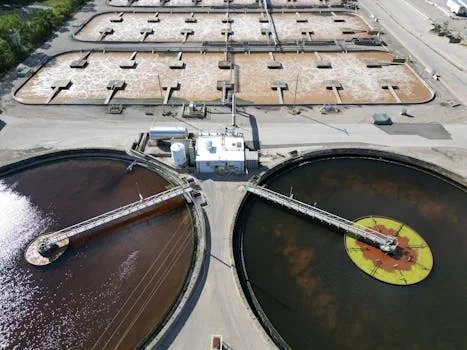
Semiconductor manufacturing processes produce complex wastewater streams containing dissolved metals like copper, high concentrations of fluoride, arsenic, and strong oxidants such as hydrogen peroxide, which necessitate advanced engineering solutions beyond conventional treatment methods. For instance, Chemical Mechanical Planarization (CMP) processes generate wastewater with dissolved copper often exceeding 10 mg/L, significantly surpassing EPA discharge limits of 0.2–2 mg/L for copper (per 40 CFR 469). Similarly, Sulfuric Peroxide Mixtures (SPM) and Piranha Acid used in cleaning contain 30–50% hydrogen peroxide, requiring dedicated pretreatment to prevent degradation and fouling of sensitive downstream Reverse Osmosis (RO) membranes. Beyond these specific contaminants, semiconductor wastewater also presents challenges with fluoride concentrations ranging from 50–500 mg/L and arsenic levels typically between 1–10 mg/L. These require targeted removal systems to comply with stringent local and regional discharge standards, such as the EU Industrial Emissions Directive 2010/75/EU and China's GB 21900-2008, which often impose limits far below those for general industrial wastewater. The industry's demand for ultra-pure water (resistivity >18 MΩ·cm) for fabrication processes further drives the need for high-recovery water reuse and Zero Liquid Discharge (ZLD) systems, making them economically viable despite their substantial Capital Expenditure (CAPEX). A typical 300 mm fab producing 1,000 wafers per day can generate 200–500 m³/day of wastewater, with approximately 60% originating from CMP and various cleaning processes, highlighting the significant volume and complexity requiring specialized semiconductor wastewater engineering solutions.Contaminant-Specific Treatment Technologies and Removal Rates
Achieving stringent discharge limits and enabling water reuse in semiconductor manufacturing requires a multi-pronged approach with contaminant-specific treatment technologies, each engineered for high removal efficiencies. Effective fluoride removal from semiconductor wastewater, for example, is typically achieved through chemical precipitation using calcium chloride (CaCl₂). This method can reduce fluoride concentrations from 500 mg/L to 25–50 mg/L, representing a 90–95% reduction, but necessitates precise pH adjustment to an optimal range of pH 8–9 and generates a significant volume of calcium fluoride sludge, approximately 0.5–1 kg per cubic meter of treated wastewater. Arsenic removal in semiconductor fabs often employs coagulation with ferric chloride (FeCl₃) at a dosing rate of 30–50 mg/L, effectively removing 95% of arsenate (As(V)) and reducing concentrations from 10 mg/L to below 0.5 mg/L. However, if arsenic is present as arsenite (As(III)), a pretreatment oxidation step is crucial to convert it to the more easily precipitated As(V); common oxidation methods include chlorine, ozone, or permanganate. For dissolved copper removal from CMP wastewater, electrochemical systems offer a highly efficient and sustainable solution. These systems, operating at current densities of 100–300 A/m², can remove 99% of dissolved copper, reducing concentrations from 10 mg/L to less than 0.1 mg/L, with the added benefit of recovering copper as pure metal and eliminating sludge generation. Hydrogen peroxide destruction in SPM wastewater is critical for protecting downstream membranes. Catalytic decomposition, often using manganese dioxide (MnO₂) or advanced oxidation processes like UV/H₂O₂, achieves a 99% reduction of hydrogen peroxide, bringing concentrations down from 30% to below 0.3% within 30–60 minutes. For a flow rate of 10 m³/h, a reactor volume of 5–10 m³ would typically be required to ensure adequate contact time. Finally, acid waste neutralization is a fundamental step, where automated PLC-controlled chemical dosing systems, such as Zhongsheng’s Chemical Dosing System, adjust pH from highly acidic (pH 1–2) to a neutral range (pH 6–9) using bases like NaOH or Ca(OH)₂. Dosing ratios typically range from 0.5–1 kg of NaOH per cubic meter of wastewater to raise the pH from 1 to 7.| Contaminant | Treatment Technology | Removal Rate / Efficiency | Key Engineering Parameters | Byproducts / Notes |
|---|---|---|---|---|
| Fluoride (50-500 mg/L) | Chemical Precipitation (CaCl₂) | 90–95% reduction (to 25–50 mg/L) | pH 8–9, CaCl₂ dosing (stoichiometric) | 0.5–1 kg sludge/m³ treated |
| Arsenic (1-10 mg/L) | Coagulation (FeCl₃) | 95% reduction As(V) (to <0.5 mg/L) | FeCl₃ 30–50 mg/L; As(III) requires oxidation | Hydroxide sludge |
| Copper (10 mg/L) | Electrochemical Recovery | 99% reduction (to <0.1 mg/L) | Current density 100–300 A/m² | Pure copper metal (no sludge) |
| Hydrogen Peroxide (30%) | Catalytic Decomposition (MnO₂) / UV/H₂O₂ | 99% reduction (to <0.3%) | 30–60 min reaction time; Reactor sizing for 10 m³/h | Minimal byproducts |
| Acid Waste (pH 1-2) | Automated Neutralization (NaOH/Ca(OH)₂) | pH 1–2 to 6–9 | 0.5–1 kg NaOH/m³ (for pH 1→7) | Neutralized salts |
Zero Liquid Discharge (ZLD) vs. Water Reuse: Engineering Specs and Cost Comparison
| Feature | Zero Liquid Discharge (ZLD) | Water Reuse (MBR + RO) |
|---|---|---|
| Water Recovery Rate | 90–95% | 70–85% |
| CAPEX (for 500 m³/day) | $5–10 Million | $2–5 Million |
| OPEX (per m³ treated) | $1.0–2.0 (Energy: 10–15 kWh/m³; Chemicals: $0.5–1/m³) | $0.7–1.5 (Energy: 3–5 kWh/m³; Membrane Cleaning: $0.3–0.7/m³) |
| Footprint (for 500 m³/day) | 200–400 m² | 100–200 m² |
| Primary Technologies | Multi-stage evaporation, crystallizers, dryers | MBR, UF, RO, activated carbon |
| Key Advantage | Eliminates liquid discharge, maximizes water savings | Lower initial investment, moderate water savings |
| Key Challenge | High energy consumption, complex operation, high CAPEX | Requires robust pretreatment, residual discharge volume |
How to Select the Right Semiconductor Wastewater Engineering Solution: A Decision Framework
Selecting the optimal semiconductor wastewater engineering solution requires a structured decision framework that aligns treatment capabilities with specific fab requirements, regulatory obligations, and economic realities.- Step 1: Characterize Wastewater Streams. Begin by thoroughly characterizing all wastewater streams generated within the fab. This involves detailed analysis of volume, contaminant types (e.g., copper, fluoride, arsenic, hydrogen peroxide), their concentrations, and variability over time. Implementing 24-hour composite sampling for critical streams like CMP wastewater provides an accurate representation of the average contaminant load, while grab samples can identify peak concentrations. Understanding flow rates and chemical compositions from different process areas (e.g., CMP, cleaning, etching) is crucial for designing targeted pretreatment.
- Step 2: Define Treatment Goals. Clearly articulate the primary treatment goals. These may include strict compliance with discharge limits (e.g., Taiwan EPA: copper < 2 mg/L, fluoride < 15 mg/L; China: arsenic < 0.5 mg/L), achieving a specific level of water reuse (e.g., 70% or 90% recovery), or the economic recovery of valuable metals like copper. Sustainability initiatives and corporate environmental targets (e.g., reducing water footprint, achieving net-zero emissions) should also be integrated into these goals.
- Step 3: Evaluate Technology Fit. Assess which technologies best address the identified contaminants and goals. For example, electrochemical systems are highly effective for copper recovery with minimal sludge, making them ideal for fabs with high copper discharge. ZLD systems are best suited for water-scarce regions or facilities aiming for maximum water recovery and elimination of discharge fees, despite their higher energy demands. Conversely, an integrated MBR system combined with a high-recovery RO system offers a balanced approach for significant water reuse at a lower CAPEX. Consider the pros and cons of each technology in the context of your fab's specific contaminant profile and operational constraints.
- Step 4: Assess CAPEX/OPEX Trade-offs. Conduct a comprehensive financial analysis comparing the Capital Expenditure (CAPEX) and Operational Expenditure (OPEX) of the shortlisted solutions. A cost calculator template can be invaluable here: for instance, compare a ZLD system with an estimated $5M CAPEX and $0.8/m³ OPEX against an MBR + RO system with $2M CAPEX and $0.5/m³ OPEX. Factor in potential savings from water reuse, reduced discharge fees, and recovered materials to calculate the Return on Investment (ROI) and total cost of ownership over the system's lifespan.
- Step 5: Pilot Test Top 2–3 Solutions. Before full-scale implementation, conduct pilot testing for the top two or three most promising solutions. Pilot programs, typically lasting 3–6 months, provide real-world data on key performance metrics such as actual contaminant removal rates, energy consumption, chemical dosing requirements, membrane fouling rates, and sludge production under the fab's specific wastewater conditions. This critical step mitigates risk and validates performance before significant investment.
Emerging Solutions: Printed Electronics and Minimal Liquid Discharge (MLD)
Frequently Asked Questions
What are the discharge limits for semiconductor wastewater?
Discharge limits for semiconductor wastewater vary by region but are generally very stringent. The U.S. EPA (40 CFR 469) limits copper to 2 mg/L, fluoride to 20 mg/L, and requires pH to be maintained between 6–9. Local regulations can be even stricter; for example, Taiwan EPA sets limits for fluoride at < 15 mg/L, and China's national standards mandate arsenic concentrations below 0.5 mg/L.
How much does a semiconductor wastewater treatment system cost?
The Capital Expenditure (CAPEX) for a semiconductor wastewater treatment system can range significantly, typically from $2 million for a Medium-recovery Water Reuse system (e.g., MBR + RO for 500 m³/day) up to $10 million for a Zero Liquid Discharge (ZLD) system of the same capacity. Operational Expenditure (OPEX) generally falls between $0.5–1.5/m³ of treated wastewater, largely dependent on energy costs, chemical consumption, and sludge disposal fees.
Can hydrogen peroxide in SPM wastewater damage RO membranes?
Yes, hydrogen peroxide (H₂O₂) in Sulfuric Peroxide Mixtures (SPM) wastewater can severely damage polyamide Reverse Osmosis (RO) membranes. H₂O₂ is a strong oxidant that degrades the membrane material, leading to increased permeability, reduced salt rejection, and premature membrane failure. Effective pretreatment, such as catalytic decomposition using manganese dioxide or advanced oxidation processes like UV/H₂O₂ followed by activated carbon filtration, is required to reduce H₂O₂ concentrations to below 1 mg/L before the wastewater enters the RO system.
What is the best solution for copper recovery from CMP wastewater?
Electrochemical systems are generally considered the most effective solution for copper recovery from Chemical Mechanical Planarization (CMP) wastewater. These systems can achieve 99% removal of dissolved copper, recovering it as pure metallic copper. This process not only ensures compliance by reducing copper discharge but also eliminates the generation of hazardous sludge, which can cost $50–100/ton to dispose of, thereby offering significant operational cost savings.
How do ZLD systems handle high-TDS wastewater from semiconductor fabs?
Zero Liquid Discharge (ZLD) systems are specifically designed to handle and process high-TDS (Total Dissolved Solids) wastewater from semiconductor fabs. They typically employ multi-stage evaporation technologies, such as mechanical vapor recompression (MVR) evaporators, to concentrate the dissolved solids. This process can increase TDS levels to over 200,000 mg/L, after which crystallizers are used to recover solid salts. While highly effective, these systems are energy-intensive, consuming 10–15 kWh/m³ of treated water, primarily for the thermal separation processes.
Related Equipment
The following Zhongsheng Environmental products are engineered for the wastewater challenges discussed above:
- PLC-controlled chemical dosing system for pH adjustment and contaminant precipitation — view specifications, capacity range, and technical data
- Integrated MBR system for high-quality effluent and water reuse — view specifications, capacity range, and technical data
- High-recovery RO system for semiconductor water reuse and ZLD pretreatment — view specifications, capacity range, and technical data
Need a customized solution? Request a free quote with your specific flow rate and pollutant parameters.