Why Semiconductor Fabs Can't Afford Water Quality Failures
Semiconductor ultrapure water treatment feeds wafer cleaning tools that need resistivity above 18.2 MΩ·cm, total organic carbon (TOC) below 1 ppb, and dissolved silica below 0.5 ppb at the point of use (POU). Modern fabs meet these limits with a three-stage train: makeup (coagulation, multimedia filtration, reverse osmosis), primary treatment (185 nm UV for TOC reduction, membrane degasification, continuous deionization or mixed-bed ion exchange), and a polishing loop (ultrafiltration, 254 nm UV, final degasification). According to MKS Instruments, a typical 200 mm fab processing 20,000 wafers per month can use up to 3,000 m³/d (≈793,000 US gpd) of UPW. The 2015 ITRS Roadmap cited a usage target of roughly 4.5 L/cm² per wafer for 2020.
Yield loss in advanced nodes is often traced to trace ionic or organic contamination in rinse water. A 2024 case study of a 300 mm fab reported a 12% yield loss attributed to colloidal silica above 1 ppb, which produced microscopic surface defects during chemical mechanical planarization (per MKS Instruments data). At 5 nm and 3 nm, the margin is gone: a single 10 nm particle can bridge a circuit line and create a killer defect, and one failed batch can erase millions of dollars in revenue. Water is the primary cleaning fluid across dozens of FEOL and BEOL steps, so any chemistry swing forces tool downtime. UPW reliability is therefore a fab profitability control, not a utility afterthought.
By 2026, advanced fabs must hold resistivity at the theoretical 18.2 MΩ·cm ceiling and TOC below 1 ppb to protect gate oxide integrity. One large fab can draw as much water as a small city, which pushes operators toward reclaim and recycle. That recovered water still has to clear the same polishing-loop purity specs.
Ultrapure Water Treatment Stages: Process Flow and Engineering Specs
Semiconductor ultrapure water production from raw feed to 18.2 MΩ·cm UPW runs through makeup, primary treatment, and a continuously circulating polishing loop. In makeup, coagulation and multimedia filtration drive the Silt Density Index (SDI) below 3 and turbidity below 0.1 NTU, the envelope reverse osmosis (RO) membranes need to survive. RO systems for semiconductor UPW pretreatment are typically configured in two-pass arrays to remove roughly 98% of dissolved ions and 99% of organics before primary treatment. Granular activated carbon (GAC) ahead of the RO strips free chlorine and a share of low-molecular-weight organics that would otherwise oxidize or foul the polyamide membrane. Filter media selection and backwash interval matter: media that slips past SDI 3 will quietly destroy RO throughput within a quarter.
The primary stage moves water from pure to ultrapure by targeting molecular contaminants RO cannot reject. TOC-reduction UV lamps at 185 nm photo-oxidize organics into CO₂ and water, membrane degasifiers drop dissolved oxygen (O₂) below 10 ppb, and continuous deionization (CDI) or mixed-bed resin polish resistivity above 17 MΩ·cm. In the polishing loop, 0.001 µm ultrafiltration removes the last particles and bacteria, high-intensity 254 nm UV and a final degasifier hold the 2026 ITRS-aligned targets of <1 ppb TOC and <0.5 ppb silica at POU, and precise chemical dosing for UPW pH adjustment and disinfection keeps rejection rates and CDI kinetics on target. Distribution is not a passive pipe run: PVDF or PFA loops with controlled velocity avoid dead legs where biofilm or particles could accumulate, and online monitors at multiple points feed real-time signals back to the fab control platform.
| Process Stage | Key Technology | Target Parameter | 2026 Engineering Limit |
|---|---|---|---|
| Makeup (Pretreatment) | Multi-media / RO / GAC | SDI / Turbidity / Chlorine | SDI < 3.0; Turbidity < 0.1 NTU; Chlorine < 0.1 ppm |
| Primary Treatment | 185nm UV / Membrane Degasification / CDI | Resistivity / O₂ / TOC | > 17.5 MΩ·cm; O₂ < 5 ppb; TOC < 2 ppb |
| Polishing Loop | Ultrafiltration / 254nm UV / Final Degasification | Particles / Silica / Bacteria | < 10 particles/mL (@ 0.05μm); Silica < 0.5 ppb; Bacteria < 1 CFU/mL |
| Distribution | PVDF / PFA Piping / Point-of-Use Filters | TOC / Boron / Particles at POU | TOC < 1 ppb; Boron < 0.1 ppb; < 5 particles/mL (@ 0.02μm) at POU |
The sections that follow map the parameters fabs actually measure, compare the two dominant deionization paths, and lay out a selection checklist for sizing a UPW train.
Key Parameters and Monitoring: What Fabs Measure and Why
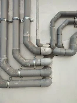
Resistivity at 18.2 MΩ·cm is the baseline indicator, but the sensor behind the number matters. High-precision conductivity probes with integrated temperature compensation are standard, because a 0.1 °C drift at the cell can mask a real ionic breakthrough. TOC monitoring runs alongside on online UV persulfate oxidation or high-temperature combustion analyzers; organics that survive to the wafer carbonize during high-temperature anneal steps and form non-conductive islands that show up as open-circuit failures at 5 nm. Analyzer selection is not a commodity call: faster TOC response shortens the gap between a chemistry excursion and a tool alarm.
Silica and boron decide whether a polishing train is adequate for 2026 specs. Silica must stay below 0.5 ppb, or it precipitates as glass-like deposits during drying and roughens the wafer surface. Boron, which slips past standard RO rejection curves, must stay below 0.1 ppb so p-type doping stays in control and transistor threshold voltage does not drift. Dissolved oxygen is held below 5 ppb to prevent uncontrolled oxidation of sensitive surfaces during critical cleans; electrochemical or optical DO sensors feed the membrane degasifier controls. The monitoring stack feeds a centralized fab control platform so one excursion triggers automated valve action instead of a delayed batch scrap.
| Parameter | 2026 Target (ITRS) | Monitoring Method | Impact of Failure |
|---|---|---|---|
| Resistivity | > 18.2 MΩ·cm | Online Conductivity with Temp. Compensation | Ionic contamination, altered transistor performance, leakage currents |
| TOC | < 1 ppb | Online UV Persulfate Oxidation / Combustion | Organic residue, gate oxide defects, film uniformity issues |
| Dissolved Silica | < 0.5 ppb | Colorimetric / Inductively Coupled Plasma (ICP) | Surface scaling, CMP defects, particle generation |
| Boron | < 0.1 ppb | ICP-MS (Lab) / ICP-OES (Online) | Unintentional p-type doping shift, threshold voltage variations |
| Dissolved O₂ | < 5 ppb | Optical / Electrochemical Sensors | Uncontrolled oxidation of wafer surface, oxide integrity issues |
| Particles | < 10 particles/mL (@ 0.05μm) | Laser Particle Counters | Surface defects, short circuits, pattern collapse |
CDI vs Mixed Bed Deionization: Performance, Costs, and Use-Case Matching
Continuous Deionization (CDI) systems deliver roughly 30% higher removal of weakly ionized species like silica and boron than traditional mixed-bed ion exchange, and they avoid the acid and caustic regeneration cycle entirely. In a 300 mm fab, the absence of rinse-up spikes during resin exhaustion tips the choice: product quality stays flat across a campaign instead of dipping when a mixed bed nears its endpoint. Capital cost and operating cost tell different stories. A 100 m³/h CDI train runs about $350,000 in CapEx versus about $200,000 for a mixed-bed system, yet OpEx swings the other way. Mixed beds consume $0.10–$0.30/m³ in chemicals, while CDI OpEx is essentially electricity and membrane replacement, typically below $0.05/m³. Removing acid and caustic from the site also cuts neutralization load and waste-handling exposure.
Mixed-bed deionization still has a role at 200 mm fabs and legacy nodes where silica below 1 ppb is acceptable. Over the lifecycle, resin replacement and regeneration drive mixed-bed OpEx to $0.50–$0.80/m³ of produced water, which pushes high-volume 300 mm fabs toward CDI and a 3–5 year ROI through chemical savings and added tool uptime. The non-obvious catch with CDI is pretreatment discipline: turbidity and SDI must stay below 1 to keep ion-exchange membranes from fouling, and that pushes responsibility upstream onto the makeup stage. Most plants we size for 300 mm conversion run polished-water TOC at the lower end of the 1 ppb envelope because the CDI does the final polish, not the mixed bed. For smaller fabs where capital is the binding constraint and quality swings are tolerable, mixed beds remain defensible, but the wastewater side then matters, and an Underground Package Sewage Treatment Plant (WSZ Series) is often specified to handle the regeneration neutralization stream without taking floor space above grade.
Equipment Selection Checklist for UPW Trains
A practical selection sequence for a 2026-era UPW train looks like this:
- Source water audit: confirm feed TOC, silica, boron, and free chlorine before sizing GAC and RO.
- Pretreatment envelope: SDI < 3, turbidity < 0.1 NTU, chlorine < 0.1 ppm at the RO inlet.
- RO pass count: two-pass array for ≥98% ion rejection and ≥99% organic rejection before primary treatment.
- Primary deionization choice: CDI for 300 mm and ≥5 nm nodes where OpEx dominates; mixed bed for legacy nodes with CapEx constraints.
- Polishing loop: 0.001 µm UF, 254 nm UV, final degasifier, with POU filters rated for <5 particles/mL at 0.02 µm.
- Materials of construction: PVDF or PFA distribution loop, welded joints, documented flush and rinse-up procedure.
- Monitoring stack: temperature-compensated resistivity, online TOC, ICP-based silica and boron checks, laser particle counters at POU.
Cost Drivers Across a 20-Year Lifecycle
The line items that swing UPW total cost of ownership are feed organics concentration, silica and boron load, electricity tariff, and regeneration chemistry on the deionization step. UPW capital is dominated by RO trains, CDI or mixed-bed skids, the polishing loop with UF and UV, and PVDF or PFA distribution; operating cost is dominated by RO membrane replacement, CDI membrane and electricity, mixed-bed resin and chemicals, and the energy to keep loop velocity above the biofilm threshold. Treating the polishing loop and any regeneration neutralization through a packaged Underground Package Sewage Treatment Plant (WSZ Series) keeps the above-grade footprint small and simplifies permitting on constrained sites. A 20-year model should track energy and chemical indices plus the cost of quality excursions, since one batch of contaminated wafers can offset several years of utility savings.
Who This Guide Is For
Process engineers and EPC contractors sizing greenfield UPW trains for 300 mm fabs, plant managers evaluating CDI retrofits at operating sites, and procurement leads comparing deionization technologies on lifecycle cost will find the specs, tables, and selection checklist directly applicable. Teams focused on fab wastewater rather than the UPW loop, or buyers looking for a packaged biological treatment skid sized in m³/d rather than a high-purity polishing train, should look at adjacent process pages instead. For a site-specific CapEx and OpEx compare on your feed analysis and node target, request a UPW train quote.
Frequently Asked Questions
What purity does semiconductor UPW actually need in 2026? Resistivity above 18.2 MΩ·cm, TOC below 1 ppb, dissolved silica below 0.5 ppb, boron below 0.1 ppb, dissolved oxygen below 5 ppb, and fewer than 10 particles/mL at 0.05 µm at the point of use. These are the ITRS-aligned targets for advanced nodes and they apply at POU, not at the polishing skid outlet.
How much does a 100 m³/h UPW deionization train cost to buy and run? A CDI system at 100 m³/h runs about $350,000 in CapEx versus about $200,000 for a mixed-bed system, but mixed-bed OpEx is $0.10–$0.30/m³ in chemicals plus $0.50–$0.80/m³ over the full lifecycle, while CDI OpEx stays below $0.05/m³ in electricity and membrane service.
What drives the 20-year lifecycle cost of a UPW system? Feed-water organic and silica load, electricity price, RO and CDI membrane replacement cadence, mixed-bed resin and regeneration chemistry, and the energy to keep the polishing loop above biofilm-threshold velocity. Add the cost of a single batch scrap from an undetected excursion and quality risk starts to dominate the model.
When should a fab pick mixed-bed over CDI? Mixed beds remain a defensible choice at 200 mm fabs and legacy nodes where silica below 1 ppb is acceptable, capital is the binding constraint, and the site is set up to handle acid and caustic regeneration safely. For 300 mm and ≥5 nm nodes, CDI usually wins on lifecycle cost.
How much flow margin should the UPW loop carry for fab expansion? Sizing the polishing loop at 110–125% of current peak demand, with RO and CDI trains on modular skids that can be added in parallel, covers a typical node-to-node ramp without forcing a full rebuild of the distribution piping.
Related Equipment
The following HydropureWater products are engineered for the wastewater challenges discussed above: