Chip Fab Wastewater Treatment Equipment: 2026 Engineering Specs, Zero-Fouling Design & Cost Benchmarks
Unplanned downtime due to fouled membranes in wastewater treatment systems can halt semiconductor fabrication, costing millions in lost production. Chip fab wastewater treatment equipment must therefore reliably handle ultra-high-purity (UPW) reject streams, hydrofluoric acid, and trace metals at parts-per-billion levels, all while enabling 70–90% water reuse. In 2026, modular systems like membrane bioreactors (MBR) and reverse osmosis (RO) dominate, achieving 92–98% COD removal and 99% TSS reduction at 10–20 LMH flux. Capital expenditure (CapEx) for these advanced systems ranges from $1.2M–$5M for 100–600 GPM facilities, with operational expenditure (OPEX) primarily driven by membrane replacement ($0.15–$0.30 per 1,000 gallons treated) and precise chemical dosing for pH adjustment and metal precipitation.Why Chip Fab Wastewater Is the Toughest Industrial Stream in 2026
Chip fabrication facilities generate 2–3 times more wastewater than their process needs due to the extensive production of ultra-high-purity (UPW) and subsequent reject streams, making its treatment one of the most complex industrial challenges (Top 1 data). Unlike conventional industrial effluent, semiconductor wastewater is defined by its extreme sensitivity, high purity requirements, and the presence of highly specialized, often hazardous, chemical contaminants. These include hydrofluoric acid (HF), tetramethylammonium hydroxide (TMAH), and trace metals such as copper (Cu) and nickel (Ni) at parts-per-billion (ppb) levels, which demand sophisticated and targeted removal strategies (Top 3 data). Legacy wastewater treatment systems frequently struggle with the unique characteristics of chip fab streams. They are prone to severe fouling from organic polymers, silica scaling, and metal precipitates, leading to frequent operational disruptions. Such issues commonly result in 12–24 hours of unplanned downtime per month for maintenance and cleaning, significantly impacting production schedules and operational costs. the semiconductor industry faces stringent regulatory pressures, including EPA 40 CFR 469 in the U.S. and the EU Industrial Emissions Directive 2010/75/EU, which dictate strict discharge limits for various pollutants. Local water scarcity mandates, such as Taiwan’s ambitious 2025 water reuse targets, also compel fabs to invest in advanced water recovery and reuse technologies, further elevating the complexity of semiconductor wastewater treatment.Chip Fab Wastewater Streams: Composition, Flow Rates, and Treatment Challenges
UPW reject streams, originating from the production of ultrapure water, typically have low organic content (1–5 mg/L TOC) and low turbidity (<10 NTU) but can exhibit conductivity ranging from 50–200 µS/cm. These streams represent a significant volume, often contributing 2–10 GPM per tool, accumulating to hundreds or thousands of GPM fab-wide, making them prime candidates for RO systems for UPW recovery and reuse.
Hydrofluoric acid (HF) wastewater, primarily from etching processes, presents a severe challenge with fluoride concentrations ranging from 100–5,000 ppm and a highly acidic pH of 2–4. Effective treatment requires precise calcium hydroxide (Ca(OH)₂) dosing at a 1.2:1 molar ratio to precipitate fluoride as calcium fluoride, a strategy proven in various applications (Top 2 case study).
TMAH wastewater, from developers and strippers, is characterized by high pH (12–14) and TMAH concentrations of 50–200 ppm. While TMAH is biodegradable, its high concentration and alkalinity can be toxic to conventional biological treatment systems, necessitating pH adjustment and specialized biological or ion exchange processes for TMAH removal.
CMP (chemical mechanical planarization) wastewater contains high levels of suspended solids and silica, typically 100–1,000 mg/L silica and 50–500 mg/L TSS. These streams require robust pre-treatment, such as lamella clarifiers or dissolved air flotation (DAF), to prevent downstream fouling (Top 1 data).
Cooling tower blowdown, while less chemically complex, contains elevated total dissolved solids (500–2,000 mg/L TDS) and phosphates (10–50 mg/L). This stream is often treated with RO systems or electrocoagulation to recover water and reduce discharge volume.
| Wastewater Stream | Key Contaminants | Typical Concentration Range | pH Range | Primary Treatment Challenge |
|---|---|---|---|---|
| UPW Reject | TOC, Conductivity | 1–5 mg/L TOC, 50–200 µS/cm | Neutral | Low concentration, high volume, high reuse potential |
| Hydrofluoric Acid (HF) | Fluoride | 100–5,000 ppm | 2–4 (acidic) | Heavy metal and fluoride precipitation |
| TMAH | TMAH | 50–200 ppm | 12–14 (alkaline) | Biodegradability, pH neutralization |
| CMP | Silica, TSS | 100–1,000 mg/L SiO₂, 50–500 mg/L TSS | Neutral | High solids, colloidal silica removal, fouling |
| Cooling Tower Blowdown | TDS, Phosphate | 500–2,000 mg/L TDS, 10–50 mg/L PO₄³⁻ | 7–9 | TDS reduction, scaling prevention |
Treatment Technologies for Chip Fab Wastewater: Engineering Specs and Performance Benchmarks
Modern chip fabrication facilities rely on a suite of advanced wastewater treatment technologies, each engineered to achieve specific removal efficiencies and enable high levels of water reuse. Selecting the optimal technology depends on the specific influent characteristics, desired effluent quality, and water reuse objectives.MBR (Membrane Bioreactor) systems for semiconductor wastewater are highly effective for streams with organic content, achieving 99% TSS removal and 92–97% COD removal. These systems typically operate at a flux rate of 10–20 LMH (liters per square meter per hour) and boast a membrane lifespan of 12–24 months, largely due to integrated fouling mitigation strategies like vigorous air scouring (Zhongsheng field data, 2025). The compact footprint and high effluent quality make MBR ideal for treating wafer cleaning wastewater.
RO systems for UPW reject and cooling tower blowdown are essential for high-purity water recovery, capable of achieving 95–98% TDS removal with a typical water recovery rate of 70–85%. RO membranes operate at a flux of 15–25 LMH and require careful pre-treatment and anti-scalant dosing at 2–5 mg/L to prevent scaling, particularly from silica and hardness (Top 1 data). Proper RO membrane lifespan and zero-fouling design for etching wastewater are critical for sustained performance.
Ion Exchange (IX) systems are highly specialized for removing specific ions, achieving >99% metal removal for contaminants like copper (Cu) and nickel (Ni). Resin capacities typically range from 1–3 eq/L, and regeneration is performed using 4–6% HCl or NaOH. Specialized resins can also be employed for effective TMAH removal, offering a non-biological alternative for highly alkaline streams.
Chemical Precipitation is a foundational treatment for specific contaminants. With calcium hydroxide (Ca(OH)₂), 95% fluoride removal can be achieved in hydrofluoric acid wastewater. For heavy metals, sodium sulfide (Na₂S) can achieve >90% metal removal. While effective, this process generates significant sludge, typically 5–10% of the influent volume (Top 2 case study).
Electrocoagulation (EC) offers a robust solution for challenging streams, demonstrating 80–90% silica removal and 70–80% TOC removal. Energy consumption for EC systems ranges from 0.5–1.5 kWh/m³, depending on the influent characteristics and desired effluent quality. The process uses sacrificial electrodes (e.g., aluminum or iron) to destabilize contaminants, which then aggregate and can be removed by sedimentation or filtration.
| Technology | Key Contaminants Targeted | Typical Removal Rate | Operating Flux / Capacity | Key Dosing / Energy | Typical Application |
|---|---|---|---|---|---|
| MBR | TSS, COD, BOD | 99% TSS, 92–97% COD | 10–20 LMH flux | Air scouring (2–5 m³/m²·h) | Wafer cleaning, general fab wastewater |
| Reverse Osmosis (RO) | TDS, Ions, Organics | 95–98% TDS, 70–85% recovery | 15–25 LMH flux | Anti-scalant (2–5 mg/L) | UPW reject, cooling blowdown, water reuse |
| Ion Exchange (IX) | Metals (Cu, Ni), TMAH | >99% metals, >95% TMAH | 1–3 eq/L resin capacity | Regeneration with 4–6% HCl/NaOH | Trace metal removal, specific ion polishing |
| Chemical Precipitation | Fluoride, Heavy Metals | 95% Fluoride, 90% Metals | Batch or continuous flow | Ca(OH)₂, Na₂S dosing | HF wastewater, metal-laden streams |
| Electrocoagulation (EC) | Silica, TOC, TSS | 80–90% Silica, 70–80% TOC | 0.5–1.5 kWh/m³ energy | Sacrificial electrodes (Al, Fe) | CMP wastewater pre-treatment, challenging organics |
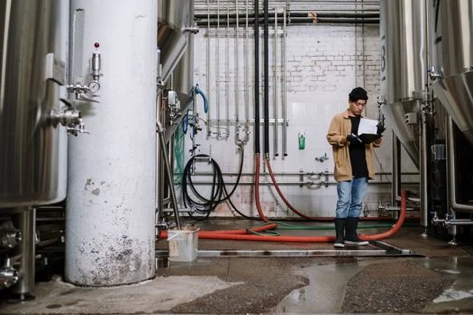
Zero-Fouling Design: How to Prevent Downtime in Semiconductor Wastewater Systems
Modular vs. Centralized Systems: CapEx, OPEX, and ROI for Chip Fabs
Modular wastewater treatment systems offer 12-18 month lead times and CapEx ranging from $1.2M–$3M for 100–300 GPM facilities, providing rapid deployment advantages over larger centralized plants. The decision between a modular and a centralized wastewater treatment system for a chip fabrication plant involves a complex evaluation of capital expenditure (CapEx), operational expenditure (OPEX), project lead times, and long-term return on investment (ROI). Each approach presents distinct financial and operational trade-offs that align with different fab sizes, expansion strategies, and water reuse goals.Modular systems, often pre-engineered and skid-mounted, offer significant flexibility and scalability. Their CapEx typically ranges from $1.2M–$3M for systems treating 100–300 GPM, with OPEX averaging $0.20–$0.40 per 1,000 gallons treated. A major advantage is their expedited lead time, usually 12–18 months from order to operation, enabling rapid response to production demands or phased expansions. This allows fabs to match treatment capacity precisely to current needs, deferring larger capital outlays until necessary.
In contrast, centralized systems are custom-built, large-scale installations designed to handle higher flow rates. CapEx for centralized facilities can range from $3M–$8M for systems treating 500–2,000 GPM, though OPEX can be slightly lower, typically $0.10–$0.25 per 1,000 gallons, due to economies of scale (Zhongsheng field data, 2025). However, their implementation involves a longer lead time, often 24–36 months, encompassing extensive design, permitting, and construction phases (Top 2 case study).
The ROI for both system types is primarily driven by three factors: water reuse rates, reduced hauling costs, and avoided compliance penalties. Achieving 70–90% water recovery significantly offsets fresh water procurement costs, which can be substantial. Reduced hauling of concentrated waste streams, typically costing $0.50–$2.00 per gallon, directly improves the bottom line. avoiding regulatory fines for non-compliance, which can escalate into millions for chronic violations, represents a critical financial safeguard. A practical decision framework suggests using modular systems for fabs with flow rates less than 500 GPM or for facilities planning phased expansions where immediate capacity is needed. Centralized systems are generally more cost-effective for larger fabs exceeding 1,000 GPM, especially those operating in regions with severe long-term water scarcity, where maximizing water reuse from a single, robust facility is paramount.| Feature | Modular Systems | Centralized Systems |
|---|---|---|
| CapEx (100–2,000 GPM) | $1.2M–$3M (100–300 GPM) | $3M–$8M (500–2,000 GPM) |
| OPEX (per 1,000 gallons) | $0.20–$0.40 | $0.10–$0.25 |
| Lead Time | 12–18 months | 24–36 months |
| Scalability | High (add units as needed) | Lower (requires major expansion) |
| Footprint | Smaller, distributed | Larger, concentrated |
| Best For | <500 GPM fabs, phased expansions, rapid deployment | >1,000 GPM fabs, long-term water scarcity, economies of scale |
Frequently Asked Questions
What is the typical payback period for a chip fab wastewater treatment system?
The typical payback period for a comprehensive chip fab wastewater treatment system ranges from 2–5 years. This timeframe is highly dependent on factors such as local water costs, the percentage of water reused (e.g., 70–90% recovery), and the magnitude of avoided discharge fees or compliance penalties. For instance, a system with a CapEx of $2M might save $500K annually in water and hauling costs, leading to a 4-year payback.
How do you treat hydrofluoric acid wastewater from semiconductor fabs?
Hydrofluoric acid (HF) wastewater from semiconductor fabs is primarily treated through chemical precipitation. Calcium hydroxide (Ca(OH)₂) is dosed at a 1.2:1 molar ratio to the fluoride concentration, precipitating fluoride as insoluble calcium fluoride (CaF₂). This is typically followed by a sedimentation tank or dissolved air flotation (DAF) to separate the precipitated solids, achieving effluent fluoride targets often below 10 ppm (e.g., Taiwan’s regulatory limit).
What are the key compliance standards for chip fab wastewater?
Key compliance standards for chip fab wastewater include the U.S. EPA 40 CFR 469 (Effluent Guidelines and Standards for the Electrical and Electronic Components Point Source Category) and the EU Industrial Emissions Directive 2010/75/EU. Additionally, local and regional discharge limits, such as Taiwan’s 10 ppm fluoride limit or specific heavy metal discharge caps, must be met. These regulations often dictate limits for TSS, COD, heavy metals, fluoride, and pH.
Can MBR systems handle TMAH wastewater?
Yes, MBR systems can effectively handle TMAH wastewater, achieving up to 99% TMAH removal through biological degradation. However, successful treatment requires initial pH adjustment of the highly alkaline TMAH stream to a neutral range of 7–8. An adequate hydraulic retention time (HRT) of 12–24 hours in the bioreactor is typically necessary to allow for complete biodegradation by the mixed microbial population.
What is the lifespan of RO membranes in semiconductor wastewater?
The lifespan of RO membranes in semiconductor wastewater treatment typically ranges from 3–5 years. This duration is highly dependent on effective pre-treatment to remove suspended solids, colloids, and scaling agents, as well as the consistent application of anti-scalant dosing. Regular cleaning-in-place (CIP) protocols are also crucial to mitigate flux decline rates and prolong membrane life, ensuring sustained performance and optimal water recovery.
Related Guides and Technical Resources
Explore these in-depth articles on related wastewater treatment topics: