Semiconductor Wastewater Treatment Plant: 2026 Engineering Specs, Zero-Liquid Discharge Design & Cost Benchmarks
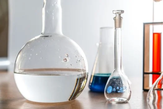
A 600 GPM semiconductor wastewater treatment plant designed for hydrofluoric acid (HF) streams requires a multi-stage treatment train to achieve zero-liquid discharge (ZLD) and meet EPA/EU discharge limits. Typical systems combine membrane bioreactors (MBR) for TMAH removal (99.9% efficiency), advanced oxidation processes (AOP) for COD elimination (92–97% at 50–500 mg/L influent), and reverse osmosis (RO) for water reuse (90–95% recovery). CapEx ranges from $5M for modular systems to $417M for full-scale ZLD plants, with OPEX driven by energy ($0.50–$2.00/m³) and chemical costs ($0.20–$1.50/m³).
Why Semiconductor Wastewater Treatment Plants Fail: 3 Hidden Design Flaws
Hydrofluoric acid (HF) corrosion in piping and pumping infrastructure accounts for 25% of mechanical failures in semiconductor wastewater facilities when material selection defaults to 316L stainless steel instead of high-nickel alloys like Hastelloy C-276. In high-concentration HF streams (typically 500–2,000 mg/L), even minor pH fluctuations cause rapid degradation of standard metallic seals and impellers. Field data from large-scale 600 GPM plants indicates that using fluoropolymer-lined piping or Hastelloy components in the primary neutralization stage extends equipment MTBF (Mean Time Between Failure) by 300% compared to standard industrial alloys.
Membrane fouling in reverse osmosis (RO) systems, driven by residual silica and organic polymers such as IPA and TMAH, can reduce water recovery rates from a design-spec 95% to below 70% within the first six months of operation. This fouling mechanism is primarily organic adsorption and colloidal scaling; silica in Chemical Mechanical Planarization (CMP) wastewater often exceeds 100 mg/L, reaching the saturation limit quickly during the concentration stages of RO. Without aggressive pre-treatment or specialized anti-scalants, the resulting flux decline necessitates frequent chemical clean-in-place (CIP) cycles, which shortens membrane lifespan from five years to less than 18 months.
Compliance violations frequently stem from inconsistent Tetramethylammonium Hydroxide (TMAH) removal, where failure to achieve 99.9% efficiency triggers EPA fines under 40 CFR Part 469, which can reach $50,000 per day. While biological treatment is the gold standard for TMAH, shock loads of photoresist stripping chemicals can inhibit microbial activity in a standard activated sludge process. energy costs for thermal evaporation systems can exceed $2.00/m³ when influent Total Dissolved Solids (TDS) exceed 10,000 mg/L, making traditional evaporation financially unsustainable compared to integrated MBR systems for semiconductor wastewater followed by high-recovery RO ($0.50–$1.00/m³).
Semiconductor Wastewater Characteristics: Influent Parameters by Process Step
Designing a resilient treatment train requires precise characterization of influent streams, as semiconductor fabrication involves highly variable chemical loads depending on the specific process step. Etching wastewater is characterized by low pH (2–4) and high fluoride concentrations (up to 2,000 mg/L), requiring specialized calcium-based precipitation before secondary treatment. In contrast, CMP wastewater presents high turbidity and Total Suspended Solids (TSS) due to abrasive slurries, requiring robust solids removal to protect downstream membranes.
| Process Step | Key Contaminants | Influent Concentration (mg/L) | pH Range | Treatment Requirement |
|---|---|---|---|---|
| Etching | Fluoride, Copper, TMAH | F: 500-2,000; Cu: 10-50 | 2.0 – 4.0 | Precipitation + MBR |
| CMP | Silica, TSS, COD | TSS: 500-2,000; Silica: 100-300 | 8.0 – 11.0 | DAF + Coagulation |
| Wafer Cleaning | IPA, Acetone, TOC | IPA: 50-200; TOC: 100-400 | 5.0 – 7.0 | AOP + RO |
| Backgrind | Silicon Particles (5-50 µm) | TSS: 1,000-5,000 | 6.5 – 8.5 | High-efficiency DAF |
For high-solids streams like backgrind and CMP waste, implementing DAF systems for high-TSS semiconductor wastewater is the most effective method for removing silicon particles and abrasive fines. This pre-treatment stage ensures that the chemical oxygen demand (COD) and TSS levels are within the acceptable range for biological reactors, preventing the "blinding" of membrane surfaces that occurs when sub-micron particles bypass traditional sand filters.
Treatment Train Design: 4 Proven Configurations for Semiconductor Wastewater
The selection of a treatment train is dictated by the balance between water reuse goals and the complexity of the influent chemistry. For facilities prioritizing sustainability, a configuration of MBR followed by RO provides 90–95% water recovery, producing effluent with COD ≤50 mg/L and TSS ≤5 mg/L. This water is typically repurposed for cooling towers or scrubbers, significantly reducing the fab's intake of municipal potable water. According to industry benchmarks, these systems consume between 1.2 and 1.8 kWh/m³ of treated water.
In regions with strict "Zero Liquid Discharge" mandates, an Advanced Oxidation Process (AOP) combined with evaporation crystallization is necessary. This configuration achieves 99% water recovery but carries a significantly higher energy footprint (4–6 kWh/m³) and CapEx ($20–$50M for a 1,000 m³/day plant). The AOP stage is critical for breaking down recalcitrant organics that would otherwise cause foaming or scaling in the multi-effect evaporators. For specific organic challenges, MBR for etching wastewater treatment has proven highly effective at removing nitrogenous compounds like TMAH with 99.9% efficiency.
| Treatment Train | Primary Objective | Recovery Rate | Energy Use (kWh/m³) | CapEx (500-1k m³/d) |
|---|---|---|---|---|
| MBR + RO | Water Reuse | 90–95% | 1.2 – 1.8 | $5M – $15M |
| AOP + Evaporation | ZLD Compliance | 99%+ | 4.0 – 6.0 | $20M – $50M |
| Chem Prep + MBR | TMAH/F Removal | 80–85% | 0.8 – 1.2 | $3M – $8M |
| DAF + MBR + RO | High-TSS Streams | 85–92% | 1.5 – 2.0 | $8M – $20M |
For facilities dealing with high-strength organics, evaporation crystallization for ZLD in semiconductor wastewater is the final barrier against environmental discharge, though it requires a robust pre-treatment stage to manage solid waste disposal costs effectively. Most modern fabs now integrate RO systems for semiconductor water reuse as a standard intermediate step to concentrate the brine before thermal treatment, thereby reducing the size and cost of the evaporation units.
Engineering Specs: Critical Parameters for Semiconductor Wastewater Treatment Equipment
MBR systems in semiconductor applications must utilize PVDF flat sheet membranes with a 0.1 µm pore size to ensure complete retention of biomass and pathogens. These membranes typically operate at a flux of 10–20 LMH (liters per square meter per hour) to balance throughput with fouling resistance. Aeration energy for these systems ranges from 0.3 to 0.5 kWh/m³, depending on the organic loading. Using PVDF flat sheet MBR membranes for semiconductor wastewater allows for aggressive chemical cleaning (pH 2–12) which is essential for removing the complex organic films typical of fab waste.
Advanced Oxidation Processes (AOP) for COD elimination require a UV-C wavelength of 254 nm and a dosage of 500–1,000 mJ/cm². When combined with hydrogen peroxide (H₂O₂), this process achieves 92–97% COD removal for influent concentrations between 50 and 500 mg/L. Chemical costs for H₂O₂ dosing typically range from $0.20 to $0.50/m³. For the final polishing of reused water, RO membranes must be polyamide thin-film composites capable of 99.5% salt rejection, operating at a flux of 15–25 LMH. These membranes have a typical lifespan of 3–5 years if pre-treatment (such as MBR or ultrafiltration) maintains a Silt Density Index (SDI) below 3.0.
| Equipment Type | Key Specification | Design Value | Operational Lifespan |
|---|---|---|---|
| MBR Membrane | Pore Size / Material | 0.1 µm / PVDF | 3 – 5 Years |
| AOP Reactor | UV Dose / Wavelength | 500-1,000 mJ/cm² / 254nm | 8,000 – 12,000 hrs (lamps) |
| RO Membrane | Salt Rejection Rate | 99.5% (Polyamide) | 3 – 5 Years |
| Evaporator | Solids in Brine | 30% – 50% | 15 – 20 Years (Vessel) |
Proper integration of RO for wafer cleaning wastewater involves precise pressure management to maintain constant flux as TDS levels fluctuate. Automated dosing systems for anti-scalants and pH adjustment are mandatory to prevent calcium fluoride scaling on the membrane surface, which can occur in seconds if fluoride levels spike above 20 mg/L in the RO feed.
CapEx and OPEX Breakdown: Cost Models for Semiconductor Wastewater Treatment Plants
Investment in semiconductor wastewater treatment is a multi-million dollar commitment where CapEx is often overshadowed by long-term OPEX. A standard MBR + RO system for a 1,000 m³/day facility requires a CapEx of $10M–$15M, but it offers a rapid ROI of 3–5 years by offsetting the high cost of purchasing and treating ultrapure water (UPW). The OPEX for this system is relatively low, at $0.50–$1.00/m³, primarily split between energy for aeration/pumping and the replacement of membrane modules every few years.
Zero Liquid Discharge (ZLD) systems represent the highest cost tier. For the same 1,000 m³/day capacity, an AOP + evaporation crystallization train can cost up to $50M in CapEx. The OPEX jumps to $1.50–$3.00/m³ due to the extreme energy requirements of thermal evaporation (typically 30–50 kWh per ton of water evaporated). However, for fabs located in water-stressed regions or those facing zero-discharge regulations, this investment is the only path to operational permitting. Chemical precipitation combined with MBR offers a middle ground for TMAH-heavy streams, with a CapEx of $3M–$8M and an OPEX of $0.40–$0.90/m³.
| System Configuration | CapEx (1,000 m³/d) | OPEX ($/m³) | Primary Cost Driver | Estimated ROI |
|---|---|---|---|---|
| MBR + RO | $10M – $15M | $0.50 – $1.00 | Energy & Membranes | 3 – 5 Years |
| ZLD (AOP+Evap) | $30M – $50M | $1.50 – $3.00 | Thermal Energy | 5 – 8 Years |
| Chem + MBR | $5M – $8M | $0.40 – $0.90 | Chemical Reagents | 2 – 4 Years |
| DAF + MBR + RO | $12M – $20M | $0.60 – $1.20 | Sludge Disposal | 4 – 6 Years |
Compliance Matrix: Global Standards for Semiconductor Wastewater Discharge
Semiconductor manufacturers must navigate a complex landscape of global and regional regulations that dictate maximum allowable concentrations for heavy metals, fluoride, and organic solvents. In the United States, EPA 40 CFR Part 469 sets the baseline, limiting fluoride to 4 mg/L and copper to 0.4 mg/L. However, local municipal limits in tech hubs like Arizona or Oregon are often significantly more stringent, particularly regarding Total Dissolved Solids (TDS) and thermal pollution.
In Taiwan, the world's most dense semiconductor manufacturing hub, the EPA has set specific limits for TMAH at ≤1 mg/L and IPA at ≤5 mg/L to protect local water bodies from nitrogen enrichment and oxygen depletion. China’s GB 31573-2015 standard is equally rigorous, requiring COD levels below 60 mg/L and ammonia nitrogen below 8 mg/L for electronic industry discharges. Meeting these standards requires a multi-barrier approach where MBR serves as the biological barrier and RO or AOP serves as the chemical/physical barrier.
| Regulation | Fluoride (mg/L) | Copper (mg/L) | TMAH (mg/L) | COD (mg/L) | TSS (mg/L) |
|---|---|---|---|---|---|
| EPA 40 CFR 469 (USA) | ≤ 4.0 | ≤ 0.4 | N/A* | N/A | ≤ 30.0 |
| EU Directive 2010/75 | ≤ 15.0 | ≤ 0.5 | N/A | ≤ 125.0 | ≤ 35.0 |
| Taiwan EPA | ≤ 15.0 | ≤ 1.0 | ≤ 1.0 | ≤ 100.0 | ≤ 30.0 |
| China GB 31573 | ≤ 10.0 | ≤ 0.5 | N/A | ≤ 60.0 | ≤ 20.0 |
| Korea WQCA | ≤ 15.0 | ≤ 0.5 | N/A | ≤ 40.0 | ≤ 20.0 |
*Note: While federal US limits do not specify TMAH, many state-level permits require 99.9% removal or concentrations < 2 mg/L.
How to Select the Right Treatment Train: A 5-Step Decision Framework
Selecting the optimal treatment configuration is a data-driven process that begins with a comprehensive influent characterization. Engineers must look beyond average values and identify peak concentrations of fluoride, TMAH, and silica, as these "spikes" are what typically cause system failure or compliance breaches. Following characterization, the five-step framework below guides the selection process:
- Step 1: Influent Characterization: Map every waste stream (Etch, CMP, Cleaning) to its specific chemical constituents. Use the influent parameters table to identify which streams require segregation (e.g., keeping high-fluoride waste separate from biological feed).
- Step 2: Define Compliance and Reuse Goals: Determine if the facility is aiming for simple discharge compliance (EPA/EU) or a sustainable reuse model. If reuse is the goal, MBR + RO is the baseline requirement.
- Step 3: Assess Water Reuse Potential: Calculate the demand for cooling tower make-up and scrubber water. If reuse demand exceeds 80% of wastewater volume, a high-recovery RO system is mandatory.
- Step 4: Compare CapEx/OPEX for Candidate Trains: Evaluate the 10-year Total Cost of Ownership (TCO). A system with lower CapEx (like chemical precipitation) may have much higher OPEX due to sludge disposal and chemical costs compared to an MBR system.
- Step 5: Pilot Testing: Conduct a 3–6 month pilot using the top two treatment candidates. Monitor flux decline in RO membranes and biomass health in the MBR under actual fab loading conditions. Pilot testing is the only way to verify specific chemical dosing rates and anti-scalant effectiveness.
Frequently Asked Questions
What is the typical recovery rate for a semiconductor wastewater treatment plant using MBR + RO?Standard systems achieve a recovery rate of 90–95%. The effluent produced typically features COD ≤50 mg/L and TSS ≤5 mg/L, making it suitable for industrial reuse in cooling towers and scrubbers. Energy consumption for this configuration ranges from 1.2 to 1.8 kWh/m³.
How much does a zero-liquid discharge (ZLD) system for semiconductor wastewater cost?For a capacity of 500–5,000 m³/day, CapEx ranges from $20M to over $400M for massive, centralized facilities. OPEX is typically $1.50–$3.00/m³, with energy consumption (4–6 kWh/m³) being the primary cost driver for the thermal evaporation components.
What are the key compliance limits for semiconductor wastewater discharge in the USA?Under EPA 40 CFR Part 469, the primary limits are fluoride ≤4 mg/L, copper ≤0.4 mg/L, and TSS ≤30 mg/L, with a pH range of 6–9. While TMAH is not federally regulated as a specific compound, most permits require 99.9% removal to meet general toxicity and nitrogen standards.
Can advanced oxidation processes (AOP) treat hydrofluoric acid (HF) wastewater?AOP is designed for organic destruction (COD/TOC) and does not remove fluoride. HF wastewater must first undergo chemical precipitation (usually with lime) to reduce fluoride to ≤50 mg/L before organics can be treated via AOP. The typical UV-C dose for semiconductor AOP is 500–1,000 mJ/cm².
What is the lifespan of MBR membranes in semiconductor wastewater treatment?With proper pre-treatment and automated cleaning cycles, PVDF flat sheet membranes (0.1 µm) have a lifespan of 3–5 years. They typically operate at a flux of 10–20 LMH. Maintaining an aeration rate of 0.3–0.5 kWh/m³ is essential to prevent irreversible fouling from organic photoresist residues.