Why Semiconductor Ultrapure Water System Costs Are Rising in 2025
A semiconductor ultrapure water system for a 300mm fab costs $8,000–$90,000 per set (CAPEX), with OPEX ranging from $0.50–$2.00/m³ depending on technology (RO+EDI vs MBR+CDI) and fab node (300mm vs 450mm). Key cost drivers include resistivity targets (18.2 MΩ·cm at 25°C per SEMI F63-0918), membrane replacement cycles (12–24 months for RO), and energy consumption (0.8–1.5 kWh/m³ for EDI). Emerging CDI systems reduce OPEX by 30% but require higher upfront investment ($120K+ for 50 m³/h).
450mm semiconductor fabs require approximately 2.5 times the ultrapure water (UPW) volume of 300mm facilities, a metric dictated by the increased surface area of the wafers and the higher rinse frequencies required for sub-5nm nodes. According to SEMI S23-0917 data, the transition from 300mm to 450mm nodes necessitates a proportional scaling of treatment capacity, often pushing facility managers toward modular, high-throughput systems to avoid catastrophic footprint expansion. This volume increase is compounded by the adoption of Extreme Ultraviolet (EUV) lithography, which has tightened water resistivity targets from the traditional 18.0 MΩ·cm to a strict 18.2 MΩ·cm at 25°C, as outlined in the updated SEMI F63-0918 compliance standards.
The global semiconductor water treatment market reached a valuation of $3.67 billion in 2024, maintaining an 8.2% CAGR since 2020. This growth is largely driven by the expansion of greenfield projects in North America and Southeast Asia, where water scarcity has turned UPW efficiency into a primary ROI driver. For procurement teams, the challenge is no longer just the initial purchase price; the total cost of ownership (TCO) is increasingly dominated by the energy and chemical intensity required to maintain "zero-particle" environments. As fabs migrate to smaller nodes, the "undocumented OPEX"—such as the cost of handling high-salinity brine or the energy penalty of maintaining high-pressure recirculation loops—can lead to budget overruns of up to 25% if not accounted for during the design phase.
Semiconductor Ultrapure Water System Components and CAPEX Breakdown
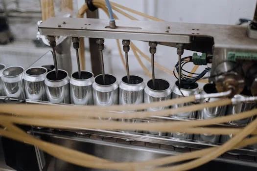
Primary reverse osmosis (RO) units represent the largest single hardware expense in the pretreatment stage, typically ranging from $2,000 to $15,000 for systems with 50–200 m³/h capacity. These units are engineered for 95–99% salt rejection, serving as the foundational barrier against dissolved solids. In high-uptime 300mm fabs, redundancy is critical; an N+1 configuration—where an extra unit is always on standby or in maintenance mode—is the industry standard, effectively increasing the baseline CAPEX for the RO stage by 30-50%. High-efficiency RO water purification systems for semiconductor fabs are essential to minimize the load on downstream polishing components.
The deionization stage has largely transitioned from traditional mixed-bed ion exchange to Electrodeionization (EDI). An EDI module costs between $3,000 and $20,000, providing a continuous, chemical-free process that yields an output of 0.1–0.3 μS/cm. While the upfront cost is higher than resin-based systems, the elimination of acid/caustic regeneration cycles makes it the preferred choice for modern facilities. Following deionization, the polishing loop—comprising UV sterilization and Total Organic Carbon (TOC) reduction units—adds another $1,500 to $10,000 to the CAPEX. These systems are designed to strip organics to levels below 1 part per billion (ppb), a requirement for preventing wafer surface contamination during the rinse cycle.
| Component | Technical Specification | Estimated CAPEX (USD) | Role in SEMI F63 Compliance |
|---|---|---|---|
| RO System | 95–99% Salt Rejection, 50-200 m³/h | $2,000 – $15,000 | Primary dissolved solids removal |
| EDI Module | Continuous regeneration, 0.1 μS/cm | $3,000 – $20,000 | Resistivity elevation to 15-18 MΩ·cm |
| Polishing Loop (UV+TOC) | <1 ppb TOC removal | $1,500 – $10,000 | Organic contaminant elimination |
| PVDF-Lined Storage | 50–500 m³ capacity, nitrogen blanketed | $500 – $5,000 | Prevents CO2 and particle re-entry |
| Distribution Piping | PVDF/PEEK, 100–500m length | $1,000 – $20,000 | Maintains 18.2 MΩ·cm to Point of Use |
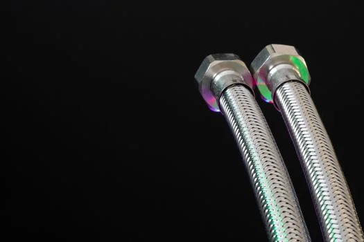
Storage and distribution infrastructure often represent "hidden" CAPEX. PVDF-lined storage tanks ($500–$5,000) and high-purity piping ($1,000–$20,000) are non-negotiable. Unlike standard industrial piping, semiconductor distribution loops must use PVDF or PEEK to prevent leaching of ions or micro-plastics into the water stream. For a 450mm fab expansion, the sheer length of these distribution lines, combined with the need for orbital welding and ultra-clean installation, can make piping costs rival the cost of the purification equipment itself.
OPEX Breakdown: Energy, Chemicals, and Maintenance Costs per m³
Energy consumption accounts for 40–60% of total operating expenses in a semiconductor water facility, with traditional RO+EDI systems consuming between 0.8 and 1.5 kWh per cubic meter of water produced. At an average industrial electricity rate, this translates to $0.08–$0.20/m³. In regions like Arizona or Singapore, where water scarcity is acute, the energy cost is often secondary to the cost of the raw water itself, but the pressure required to drive water through high-rejection membranes remains a fixed thermal and electrical load that scales with fab throughput.
Chemical costs, while smaller as a percentage of total OPEX (5–10%), are vital for system longevity. Antiscalants and cleaning agents used in pretreatment cost roughly $0.02–$0.05/m³. Precise chemical dosing for ultrapure water polishing loops is required to prevent membrane scaling and biofouling, which can prematurely end a membrane's life cycle. Membrane replacement is a significant recurring cost; RO membranes typically last 12–24 months, while EDI modules are replaced every 3–5 years. When amortized, these replacements add $0.10–$0.30/m³ to the operational budget.
| OPEX Category | Cost Range (per m³) | Key Driver | Optimization Potential |
|---|---|---|---|
| Energy (Power) | $0.08 – $0.20 | Pump pressure & EDI voltage | VFDs and CDI technology |
| Chemicals | $0.02 – $0.05 | Feed water hardness/TOC | Automated dosing precision |
| Maintenance/Membranes | $0.10 – $0.30 | Fouling rates & flux | Enhanced pretreatment (MBR) |
| Labor | $0.05 – $0.15 | Automation level | Remote monitoring/AI analytics |
| Wastewater/Brine | $0.03 – $0.10 | Local discharge fees | ZLD or water recycling loops |
Labor costs vary significantly by region and automation level. In modern 300mm fabs, highly automated systems reduce the need for manual monitoring, bringing labor costs down to $0.05/m³. However, in older facilities or those undergoing 450mm node expansions, the complexity of integrating new tech with legacy systems can increase labor to $0.15/m³ due to specialized maintenance requirements. Finally, the disposal of brine and wastewater—especially in jurisdictions with strict Zero Liquid Discharge (ZLD) mandates—can add an additional $0.03–$0.10/m³ to the total cost.
RO+EDI vs MBR+CDI: Cost and Performance Comparison for 300mm vs 450mm Fabs
Capacitive Deionization (CDI) combined with Membrane Bioreactors (MBR) represents the next frontier in semiconductor water treatment, offering a significant shift in the CAPEX/OPEX balance. While a standard RO+EDI setup for a 300mm fab might have a CAPEX of $8,000–$50,000, an MBR+CDI system can range from $30,000 to $90,000. However, the CDI system operates at much lower pressures and utilizes electrochemical regeneration rather than high-voltage EDI modules, leading to 30% lower energy consumption. For 450mm fabs, where water volume is massive, the lower OPEX of CDI ($0.35–$0.80/m³) often justifies the higher initial investment within 24–36 months.
MBR technology is increasingly used in fab water recycling loops to treat gray water for reuse in cooling towers or as influent for the UPW system. Utilizing MBR systems for semiconductor water recycling allows facilities to achieve higher recovery rates, which is critical for SEMI S23-0917 compliance. A real-world case study from a 300mm fab in Taiwan demonstrated that switching from a traditional RO-based recycling loop to a CDI-integrated system reduced overall facility OPEX by 25%, primarily through the reduction of chemical consumption and brine volume.
| Feature | RO + EDI (Traditional) | MBR + CDI (Emerging) | Benefit for 450mm Fabs |
|---|---|---|---|
| CAPEX (Relative) | Baseline (1x) | High (1.5x - 2x) | Scaling footprint is 20% smaller |
| OPEX (per m³) | $0.50 – $1.20 | $0.35 – $0.80 | Cumulative savings of $1M+/year |
| Resistivity | 18.0 – 18.2 MΩ·cm | 18.2+ MΩ·cm | Higher stability for EUV rinse |
| Chemical Usage | High (Regeneration/Cleaning) | Low (90% reduction) | Reduced hazardous waste handling |
| Water Recovery | 75% – 85% | 90% – 95% | Essential for water-stressed zones |
The primary advantage of CDI for 450mm node expansions is its ability to scale linearly with lower footprint requirements. Traditional RO systems require massive membrane housings that consume valuable cleanroom or sub-fab space. CDI stacks are more compact and can be tuned for specific ion removal, which is particularly useful when dealing with the complex wastewater profiles of integrated circuit manufacturing. For facilities managing high-salinity streams, ZLD systems for semiconductor brine management are often integrated with CDI to maximize salt recovery and minimize environmental impact.
Hidden Costs: Installation, Commissioning, and Compliance
Installation costs for a semiconductor UPW system typically account for 10–20% of the total CAPEX, ranging from $1,000 to $10,000 for standard sets. This includes the integration of the system into the fab’s existing Building Management System (BMS) and the complex task of cleanroom piping. Because UPW is highly aggressive (it will leach ions from almost any surface), the installation requires specialized technicians certified in orbital welding of PVDF. Any contamination during the installation phase can lead to weeks of flushing, delaying the start of wafer production and costing the fab millions in lost revenue.
Commissioning adds another 5–10% to the project budget. This phase involves resistivity validation, TOC testing, and ensuring the system meets SEMI F63-0918 standards. Regulatory compliance is another significant hurdle; obtaining SEMI S2 (Safety) and S8 (Ergonomics) certifications can cost between $2,000 and $10,000 depending on the system's complexity. These certifications are often required by insurance providers and local environmental agencies to ensure the system does not pose a risk to fab personnel or the local ecosystem.
Checklist: 5 Questions to Ask Suppliers About Hidden Costs
- Does the quote include the cost of initial "flushing to spec" (which can take 72+ hours)?
- Are spare parts kits for critical sensors (resistivity, TOC) included in the first year?
What is the specific cost for SEMI S2/S8 third-party certification? - Does the installation include passivating the distribution loop?
- What are the training costs for on-site engineers to manage the EDI/CDI stacks?
Geographic location also plays a role in hidden costs. For example, fab projects in California face much higher permitting and environmental impact study costs compared to projects in Texas or Arizona. Additionally, if the fab handles toxic byproducts, such as chromium from certain etching processes, the UPW system must be integrated with semiconductor wastewater treatment solutions to ensure compliance with local discharge limits, adding another layer of regulatory cost.
ROI Calculator: How Ultrapure Water Systems Impact Fab Yield and Cost per Wafer
The financial justification for investing in high-end UPW systems lies in the direct correlation between water purity and wafer yield. According to SEMI S23-0917 data, a reduction of just 1 ppb in Total Organic Carbon (TOC) can lead to a 0.5% improvement in yield for advanced logic chips. Even more significant is the impact of resistivity; maintaining a stable 18.2 MΩ·cm (vs. 18.0 MΩ·cm) has been shown in Intel whitepapers to improve yield by up to 1.2% by ensuring more complete removal of photoresist residues and ionic contaminants during the rinse phase.
To calculate the ROI of a UPW system upgrade or investment, facility managers can use the following formula: ROI = (Annual Yield Improvement × Wafer Output × Wafer ASP) / (Total CAPEX + Annual OPEX). For a 300mm fab producing 50,000 wafers per month with an average selling price (ASP) of $2,000, a 1.2% yield improvement results in $1.2 million in additional annual revenue. In this scenario, even a high-end $250,000 UPW system pays for itself in less than three months based on yield gains alone.
| Metric | 300mm Fab (Legacy UPW) | 300mm Fab (Advanced UPW) | 450mm Fab (Next-Gen) |
|---|---|---|---|
| Water Resistivity | 18.0 MΩ·cm | 18.2 MΩ·cm | 18.2+ MΩ·cm |
| TOC Levels | >5 ppb | <1 ppb | <0.5 ppb |
| Est. Yield Improvement | Baseline | +1.2% | +2.5% (vs 300mm) |
| Annual Revenue Gain | $0 | $1,200,000 | $4,500,000+ |
| Payback Period | N/A | < 6 Months | < 4 Months |
For 450mm fabs, the ROI is even more dramatic. Due to the higher ASP of 450mm wafers (often $5,000+) and the increased sensitivity of the larger surface area to contamination, the ROI on a high-spec MBR+CDI system can be 3 times higher than in 300mm facilities. Procurement teams must view the UPW system not as a utility expense, but as a critical yield-enhancement tool. Investing in superior filtration and deionization technology directly offsets the massive CAPEX of the fab's lithography and etching equipment by ensuring the highest possible "good die" count per wafer.
Frequently Asked Questions
What is the typical payback period for a semiconductor ultrapure water system?
For a 300mm fab, the payback period for a high-efficiency UPW system is typically between 6 and 18 months. This is calculated based on OPEX savings (energy and chemicals) and, more importantly, yield improvements. As demonstrated in our ROI calculator, a 1.2% yield boost can pay for the system CAPEX in a matter of months.
How does water resistivity affect EUV lithography yield?
EUV lithography uses extremely sensitive photoresists and masks. Water with resistivity below 18.2 MΩ·cm contains trace ionic impurities that can cause "staining" or "bridging" defects on the wafer surface at the sub-7nm scale. Maintaining SEMI F63-0918 standards is essential to prevent these defects and maintain high yield in EUV processes.
What are the maintenance requirements for RO membranes in a semiconductor fab?
RO membranes in a semiconductor environment require replacement every 12–24 months to maintain optimal salt rejection and flux. Regular CIP (Cleaning In Place) cycles are performed every 3–6 months using specialized antiscalants to prevent biofouling and mineral scaling, which are the primary causes of membrane failure.
Can ultrapure water systems be upgraded for 450mm fabs?
Yes, but it is rarely a simple "plug-and-play" process. Upgrading to 450mm requirements usually involves increasing the throughput of the RO/EDI stages by 2.5x and upgrading the distribution loop to handle higher flow rates while maintaining 18.2 MΩ·cm. Many fabs opt for a modular expansion where new MBR+CDI units are added in parallel to the existing system.
What are the most common failure points in semiconductor water systems?
The most common failure points are UV lamp degradation (leading to TOC spikes), EDI module scaling (reducing resistivity), and pump seal leaks in the distribution loop (introducing particles). Implementing a predictive maintenance schedule with real-time TOC and resistivity monitoring is the best way to prevent these issues from impacting fab production.