Silicon Wafer Wastewater Treatment Project: 2025 Hybrid Process Design with 99.8% Recovery & ZLD Cost Breakdown
Silicon wafer manufacturing generates 10–15 m³ of wastewater per 12-inch wafer, containing hydrofluoric acid (HF), TMAH, silicon carbide particles, and heavy metals. A 2025 hybrid treatment system—combining membrane bioreactors (MBR), advanced oxidation (AOP), reverse osmosis (RO), and chemical precipitation—can achieve 99.8% recovery and zero liquid discharge (ZLD) at a CAPEX of $1.2–2.5M for a 500 m³/day fab. Key contaminants like HF (99.9% removal via calcium precipitation) and TSS (99.8% via DAF + MBR) require tailored process trains to meet China GB 31573-2015 and EPA 40 CFR Part 469 standards.Why Silicon Wafer Wastewater Requires Specialized Treatment
Silicon wafer manufacturing operations generate highly complex and variable wastewater streams, posing significant treatment challenges due to unique contaminant profiles and stringent regulatory demands. The intricate processes involved in semiconductor fabrication, from etching to cleaning, introduce a diverse range of pollutants into the wastewater, making comprehensive treatment a critical endeavor for compliance and sustainability. The primary contaminants found in silicon wafer wastewater include:- Hydrofluoric Acid (HF): A highly corrosive acid used in etching processes, typically present at influent concentrations of 50–500 mg/L.
- TMAH (Tetramethylammonium Hydroxide): A strong organic base used in anisotropic etching and photoresist stripping, with influent concentrations often ranging from 100–1,000 mg/L.
- Silicon Carbide Particles: Abrasive particles generated during wafer slicing and grinding, contributing to TSS loads of 100–500 mg/L and posing significant fouling risks. More details on these challenges are available in our guide on 2025 discharge standards for silicon carbide wastewater.
- Ammonia-Nitrogen: Originating from various cleaning solutions and process chemicals, with typical influent concentrations of 20–100 mg/L.
- Heavy Metals (e.g., Cu, Ni, Cr): Leached from process equipment or introduced from plating baths, often found at 1–50 mg/L.
| Contaminant | Typical Influent Concentration | China GB 31573-2015 (mg/L) | EPA 40 CFR Part 469 (mg/L) |
|---|---|---|---|
| pH | 2–12 | 6–9 (discharge) | 6–9 (discharge) |
| TSS | 100–500 mg/L | 70 | 30 |
| COD | 200–1,500 mg/L | 80 | N/A (often state-specific) |
| Fluoride (HF) | 50–500 mg/L | 10 | 4 (daily max) |
| TMAH | 100–1,000 mg/L | N/A (as COD/TOC) | N/A (as COD/TOC) |
| Ammonia-Nitrogen | 20–100 mg/L | 15 | N/A (often state-specific) |
| Copper (Cu) | 1–10 mg/L | 0.5 | 0.5 (daily max) |
Hybrid Process Design: MBR + AOP + RO + Chemical Precipitation
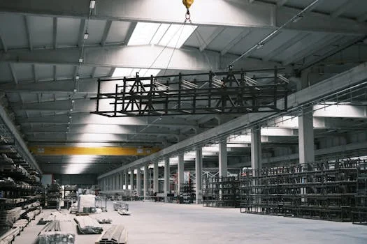
- Pretreatment: This initial stage focuses on removing suspended solids and neutralizing extreme pH. A high-efficiency DAF system for silicon carbide particle removal typically achieves 95% TSS removal. Following DAF, pH adjustment is crucial for HF neutralization, raising the pH to 7–8. This process typically requires a chemical dosing rate of 1.2 kg Ca(OH)₂ per kg of HF to effectively precipitate fluoride.
- Biological Treatment: Following pretreatment, the wastewater proceeds to a biological stage, often utilizing an MBR system for COD and ammonia-nitrogen removal in semiconductor wastewater. MBRs achieve approximately 90% COD removal and over 99% ammonia-nitrogen removal, making them highly effective for biodegradable organics. Typical membrane flux rates for wafer fab wastewater range from 15–25 LMH (liters per square meter per hour), and sludge yield is generally 0.2–0.4 kg TSS per kg COD removed (MWH Constructors, Top 1).
- Advanced Oxidation (AOP): Recalcitrant organic compounds, particularly TMAH, are not fully removed by biological treatment alone. Advanced Oxidation Processes (AOP), such as UV-AOP, are employed to achieve 99.8% COD removal for these difficult-to-degrade substances. This stage requires a UV dose of 500–1,000 mJ/cm² and H₂O₂ dosing at a 1:1 molar ratio to the remaining COD (Enviolet 2024 benchmarks, Top 4).
- Polishing: The final stage focuses on removing dissolved salts and trace contaminants to achieve water reuse or ZLD standards. An RO system for ultra-pure water recovery in ZLD applications typically achieves 99% salt rejection, with overall recovery rates ranging from 75–85%. Chemical precipitation, using sulfide or hydroxide, is then applied to remove any residual heavy metals, ensuring compliance with stringent discharge limits. The concentrated brine from the RO system can then be further treated for ZLD, while the recovered water is suitable for reuse. Sludge generated from chemical precipitation and MBR processes requires careful handling, with disposal costs often ranging from $200–400 per ton due to hazardous waste classification.
| Process Stage | Primary Function | Key Contaminants Addressed | Typical Removal Efficiency | Key Engineering Parameters |
|---|---|---|---|---|
| Pretreatment (DAF + pH Adj.) | TSS removal, HF neutralization | TSS, HF, heavy metals | 95% TSS, 99% HF | DAF: 10–20 m/h surface loading; pH: 7–8 |
| Biological Treatment (MBR) | Organic and nutrient removal | COD, BOD, Ammonia-Nitrogen | 90% COD, 99% NH₃-N | Flux: 15–25 LMH; MLSS: 8,000–12,000 mg/L |
| Advanced Oxidation (UV-AOP) | Recalcitrant organic degradation | TMAH, non-biodegradable COD | 99.8% COD (for recalcitrant) | UV Dose: 500–1,000 mJ/cm²; H₂O₂: 1:1 molar ratio to COD |
| Polishing (RO + Chemical Precip.) | Salt and trace contaminant removal | Dissolved salts, heavy metals | 99% salt rejection, >99.9% heavy metals | RO recovery: 75–85%; Precip. pH: 9–11 |
Contaminant-Specific Treatment: HF, TMAH, and Silicon Carbide
Effective silicon wafer wastewater treatment mandates targeted approaches for key contaminants like hydrofluoric acid (HF), TMAH, and silicon carbide particles, each requiring specific chemical and physical processes to ensure regulatory compliance. Understanding these contaminant-specific strategies is critical for engineers designing new systems or troubleshooting existing ones. * Hydrofluoric Acid (HF): The primary method for HF removal is calcium precipitation. This process achieves 99.9% removal by reacting HF with a calcium source, such as Ca(OH)₂, to form insoluble calcium fluoride (CaF₂). Precise pH control at 8–9 is essential for optimal precipitation. The resulting CaF₂ sludge requires dewatering, typically using a filter press for dewatering HF sludge in semiconductor wastewater treatment, before disposal. Chemical costs for HF neutralization range from $0.50–1.00/m³ of treated wastewater. A significant challenge lies in the disposal of the CaF₂ sludge, which is often classified as hazardous waste, incurring high disposal fees. Further insights into these costs are available in our detailed cost breakdown for HF wastewater treatment. * TMAH (Tetramethylammonium Hydroxide): Due to its recalcitrant nature, TMAH is best removed via UV-AOP, which achieves 99.9% removal efficiency. This process involves the generation of highly reactive hydroxyl radicals (•OH) from hydrogen peroxide (H₂O₂) under UV irradiation. Optimal H₂O₂ dosing typically follows a 1:1 molar ratio to the TMAH or COD concentration. UV lamp lifespan is generally 8,000–12,000 hours, and energy consumption for this stage ranges from 0.5–1.0 kWh/m³. Enviolet’s 2024 data (Top 4) consistently demonstrates high TMAH degradation rates with this approach. An PLC-controlled chemical dosing system for HF neutralization and TMAH oxidation is crucial for precise chemical management. * Silicon Carbide Particles: These abrasive particles pose a significant challenge due to their potential to foul membranes and wear down equipment. Effective removal relies on a combination of a high-efficiency DAF system for silicon carbide particle removal followed by ceramic membranes. This approach achieves 99.8% TSS removal. Ceramic membranes are preferred over polymeric membranes for their superior resistance to abrasion and fouling. They typically operate at higher flux rates of 50–100 LMH and require less frequent cleaning, usually 1–2 times per week with a 1% NaOH solution, compared to polymeric membranes. Saltworks Technologies, for example, designed a 600 GPM plant that effectively manages such streams (Top 3). * Heavy Metals (Cu, Ni, Cr): Chemical precipitation is the standard method for heavy metal removal. Sulfide precipitation (using Na₂S or NaHS) or hydroxide precipitation (using NaOH or Ca(OH)₂) are common. Hydroxide precipitation typically requires pH optimization to 9–11 for efficient removal. This process can reduce residual metal concentrations to below 0.5 mg/L for copper, meeting stringent EPA 40 CFR Part 469 limits. The resulting metal hydroxide or sulfide sludge is then dewatered and disposed of as hazardous waste.| Contaminant | Specific Treatment Process | Key Parameters | Removal Efficiency | Challenges/Notes |
|---|---|---|---|---|
| Hydrofluoric Acid (HF) | Calcium Precipitation | pH 8–9, Ca(OH)₂ dosing (1.2 kg/kg HF) | 99.9% | Hazardous sludge disposal, chemical costs $0.50–1.00/m³ |
| TMAH | UV-AOP | UV dose > 500 mJ/cm², H₂O₂ (1:1 molar ratio to COD) | 99.9% | Energy consumption (0.5–1.0 kWh/m³), UV lamp lifespan (8,000–12,000 hrs) |
| Silicon Carbide Particles | DAF + Ceramic Membranes | DAF 10–20 m/h, Ceramic membrane flux 50–100 LMH | 99.8% TSS | Membrane fouling, cleaning frequency (1–2x/week with 1% NaOH) |
| Heavy Metals (Cu, Ni, Cr) | Chemical Precipitation (Sulfide/Hydroxide) | pH 9–11 (hydroxide), specific precipitant dosage | >99.9% (e.g., Cu < 0.5 mg/L) | Sludge volume, hazardous waste classification |
2025 ZLD Cost Breakdown for 500 m³/day Silicon Wafer Fab
- DAF System: $150,000–250,000 (includes tanks, pumps, air saturation system)
- MBR System: $500,000–800,000 (includes tanks, membranes, blowers, controls)
- UV-AOP System: $300,000–500,000 (includes UV reactors, H₂O₂ storage and dosing)
- RO System: $200,000–400,000 (includes RO membranes, high-pressure pumps, pretreatment filters)
- Chemical Dosing System: $50,000–100,000 (for pH adjustment, coagulants, PLC-controlled chemical dosing for HF neutralization and TMAH oxidation)
- Sludge Dewatering: $100,000–200,000 (e.g., filter press for dewatering HF sludge in semiconductor wastewater treatment + polymer dosing unit)
- Total Estimated CAPEX: $1.2–2.5M
- Energy Consumption: $120,000–200,000 (based on 0.5–1.0 kWh/m³ at $0.10/kWh)
- Chemicals: $80,000–150,000 (Ca(OH)₂, H₂O₂, coagulants, polymers, acids/bases)
- Membrane Replacement: $50,000–100,000 (MBR and RO membranes every 3–5 years)
- Sludge Disposal: $40,000–80,000 (hazardous waste fees, transportation)
- Labor: $60,000–100,000 (equivalent to 1 FTE operator for monitoring and maintenance)
- Total Estimated Annual OPEX: $350,000–630,000/year
| Cost Category | CAPEX Range (USD) | Annual OPEX Range (USD) |
|---|---|---|
| DAF System | $150,000–250,000 | $15,000–25,000 (energy, minor chemicals) |
| MBR System | $500,000–800,000 | $80,000–130,000 (energy, membrane cleaning, replacement) |
| UV-AOP System | $300,000–500,000 | $100,000–180,000 (energy, H₂O₂) |
| RO System | $200,000–400,000 | $70,000–120,000 (energy, membrane cleaning, replacement) |
| Chemical Dosing | $50,000–100,000 | $10,000–20,000 (maintenance, minor energy) |
| Sludge Dewatering | $100,000–200,000 | $20,000–40,000 (energy, polymers, maintenance) |
| Total System Costs | $1,200,000–2,500,000 | $350,000–630,000 |
How to Select a Silicon Wafer Wastewater Treatment Vendor: 5 Critical Questions
Selecting the right vendor for a silicon wafer wastewater treatment project requires a structured evaluation based on five critical factors: contaminant expertise, system modularity, energy efficiency, compliance guarantees, and robust after-sales support. A thorough assessment of these areas will ensure a reliable, cost-effective, and compliant solution for your fab.- Contaminant Expertise: Does the vendor have demonstrable experience with the specific contaminants in silicon wafer wastewater? Request detailed case studies for HF, TMAH, and silicon carbide particle removal from similar projects. Crucially, ask for pilot test data based on your fab’s actual wastewater profile to validate their proposed treatment efficacy.
- Modularity: Can the proposed system adapt to variable production demands and future expansion? Inquire about the system's ability to scale efficiently, for instance, from 200 to 2,000 m³/day, without requiring a complete redesign. Modular designs, like those deployed by Saltworks Technologies for a 600 GPM plant (Top 3), offer flexibility and reduce future CAPEX.
- Energy Efficiency: What is the specific energy consumption (kWh/m³) of the proposed ZLD system? Energy is a major OPEX component, so targeting systems with consumption below 1.0 kWh/m³ for ZLD is critical. Request detailed energy audits and consumption projections for each treatment stage, especially for energy-intensive processes like AOP and RO.
- Compliance Guarantees: Does the vendor provide explicit guarantees for meeting all discharge limits (e.g., fluoride < 10 mg/L, heavy metals < 0.5 mg/L) specified by relevant regulations like China GB 31573-2015 or EPA 40 CFR Part 469? Include penalty clauses in the contract for non-compliance to protect your investment and operational continuity.
- After-Sales Support: What level of ongoing support does the vendor offer? Inquire about response times for critical issues such as membrane fouling, AOP lamp failures, or control system malfunctions. Prioritize vendors offering 24/7 remote monitoring capabilities and readily available local service teams to minimize downtime and maintain operational efficiency.
Frequently Asked Questions
Q: What’s the biggest challenge in treating silicon wafer wastewater?
A: The biggest challenges are effectively removing hydrofluoric acid (HF) and managing silicon carbide particles. HF requires precise calcium precipitation (pH 8–9) for 99.9% removal, forming a hazardous sludge. Silicon carbide particles are highly abrasive and prone to fouling membranes, necessitating robust pretreatment like DAF combined with resilient ceramic membranes to mitigate issues. Most fabs also struggle with the high sludge disposal costs, typically $200–400 per ton for hazardous waste.
Q: Can MBR systems handle TMAH (Tetramethylammonium Hydroxide)?
A: No, MBR alone achieves less than 30% TMAH removal due to its recalcitrant nature. A hybrid system combining MBR with UV-AOP is essential. This advanced oxidation process requires precise H₂O₂ dosing (typically a 1:1 molar ratio to TMAH or COD) and a substantial UV dose of > 500 mJ/cm². Enviolet’s 2024 data (Top 4) confirms that this hybrid approach can achieve 99.9% TMAH removal.
Q: What’s the payback period for a ZLD system in a silicon wafer fab?
A: The typical payback period for a ZLD system in a 500 m³/day silicon wafer fab is 3–5 years. This rapid ROI is primarily driven by significant water reuse savings ($2–5/m³) and the avoidance of substantial compliance fines ($100,000–500,000 per year) for discharge violations. While CAPEX ranges from $1.2–2.5M and OPEX from $350K–630K/year, the ROI can be further improved by the potential for recovered silicon carbide value ($50–100/ton).
Q: How do I reduce energy costs in a silicon wafer wastewater treatment system?
A: To reduce energy costs, focus on optimizing UV-AOP and RO recovery rates. Employing ceramic membranes (with higher flux rates of 50–100 LMH) instead of polymeric membranes can significantly reduce fouling and associated cleaning energy. Additionally, exploring heat recovery from RO reject streams can contribute to overall energy efficiency. The goal should be to achieve less than 1.0 kWh/m³ for ZLD systems; for example, Saltworks’ 600 GPM plant (Top 3) achieved 0.8 kWh/m³.
Q: What are the alternatives to ZLD for silicon wafer fabs?
A: An alternative to full ZLD is partial reuse (70–90% recovery). This approach typically has a lower CAPEX ($800K–1.5M) but carries the inherent risk of non-compliance if discharge limits become stricter in the future. For smaller fabs (less than 200 m³/day), onsite evaporation (e.g., using mechanical vapor recompression) can be an option, but it generally incurs very high energy costs, often 15–20 kWh/m³.