Third-generation semiconductor (GaN/SiC) fabs face discharge limits for fluoride (≤10 mg/L in China GB 8978-2024, ≤4 mg/L in EPA E&EC), arsenic (≤0.1 mg/L in China, ≤0.05 mg/L in EU), and heavy metals (e.g., copper ≤0.5 mg/L) that are 5–10x stricter than silicon fab standards. A 2025 Zero Liquid Discharge (ZLD) system combining chemical precipitation (pH 8.5–9.5 for CaF₂), MBR membrane filtration (0.1 μm PVDF), and evaporative crystallization achieves 99.9% contaminant removal while recovering 95%+ process water—critical for compliance and cost savings of $0.85–$1.20 per cubic meter treated.
Why Third-Generation Semiconductor Wastewater Fails Traditional Treatment Systems
GaN/SiC etching and substrate preparation generate fluoride at 500–2,000 mg/L, arsenic at 10–50 mg/L, and heavy metals (copper, nickel, chromium) at concentrations 10–100x higher than traditional silicon fabs, rendering conventional silicon-fab wastewater systems inadequate (HydropureWater field data, 2025). These elevated contaminant loads stem directly from the unique chemistries of third-generation semiconductor manufacturing. For instance, gallium nitride (GaN) etching frequently employs highly concentrated hydrofluoric acid (HF) and ammonium fluoride (NH₄F) mixtures, resulting in fluoride concentrations far exceeding the 50–200 mg/L typically found in silicon wafer production. Similarly, silicon carbide (SiC) substrate polishing processes utilize specific abrasives and slurries that release significant levels of colloidal silica and various heavy metals, necessitating specialized treatment approaches.
A recent case in Suzhou illustrates this challenge: a 2024 GaN fab failed to meet China GB 8978-2024 fluoride limits, discharging 12 mg/L against a 10 mg/L standard, primarily due to inadequate pH control during the chemical precipitation stage. The system, originally designed for silicon fab wastewater, maintained a pH of 7.5–8.0, which is insufficient for optimal calcium fluoride (CaF₂) precipitation, requiring a tighter range of 8.5–9.9. This highlights the critical need for precise engineering tailored to GaN/SiC contaminant profiles.
Traditional silicon-fab wastewater treatment systems commonly exhibit three critical failure modes when applied to third-generation semiconductor wastewater: (1) severe membrane fouling from the high concentrations of colloidal silica prevalent in SiC processing, leading to reduced flux and increased cleaning frequency; (2) incomplete fluoride precipitation due to insufficient pH control, as effective calcium fluoride formation requires a consistently alkaline environment (pH >8.5); and (3) arsenic breakthrough resulting from interference in co-precipitation reactions caused by high organic loads or phosphate concentrations, which are more common in GaN/SiC waste streams.
2025 Discharge Standards for Third-Generation Semiconductors: China GB 8978-2024 vs. EPA vs. EU Limits
China GB 8978-2024 sets a fluoride limit of 10 mg/L for semiconductor wastewater, while EPA E&EC (40 CFR Part 469) specifies 4 mg/L, highlighting significant jurisdictional variations that demand careful compliance planning. Understanding these differences is crucial for fabs operating globally or planning international expansion. The table below provides a side-by-side comparison of key discharge parameters:
| Parameter | China GB 8978-2024 (Semiconductor, direct discharge) | EPA E&EC (40 CFR Part 469, direct discharge) | EU IED (2010/75/EU, Microelectronics BREF) |
|---|---|---|---|
| Fluoride (F⁻) | ≤10 mg/L | ≤4 mg/L (monthly average) | ≤5 mg/L |
| Arsenic (As) | ≤0.1 mg/L | ≤0.1 mg/L (daily max) | ≤0.05 mg/L |
| Copper (Cu) | ≤0.5 mg/L | ≤0.5 mg/L (monthly average) | ≤0.2 mg/L |
| Nickel (Ni) | ≤1.0 mg/L | ≤0.5 mg/L (monthly average) | ≤0.2 mg/L |
| Chromium (Cr) | ≤1.0 mg/L (total) | ≤0.5 mg/L (total) | ≤0.1 mg/L (total) |
| Total Suspended Solids (TSS) | ≤30 mg/L | ≤30 mg/L (monthly average) | ≤10 mg/L |
| Chemical Oxygen Demand (COD) | ≤80 mg/L | N/A (regulated by local permits) | ≤50 mg/L |
| pH | 6–9 | 6–9 | 6–9 |
The strictest limits often dictate the overall treatment strategy. For instance, the EU Industrial Emissions Directive imposes a stringent arsenic limit of 0.05 mg/L, which is half of China's 0.1 mg/L, demanding more advanced polishing stages. Similarly, the EPA's fluoride limit of 4 mg/L is 2.5 times stricter than China's 10 mg/L, pushing for enhanced precipitation and membrane separation. These limits are not arbitrary; their regulatory rationale is rooted in specific environmental protection goals. China’s fluoride limit, for example, often aligns with national drinking water standards (GB 5749-2022) due to its impact on human health, while the EPA's fluoride limit is primarily based on aquatic toxicity thresholds to protect receiving water bodies (EPA 822-R-18-001). For a broader understanding of global discharge standards for microelectronics wastewater, refer to our detailed article on microelectronics wastewater discharge standards 2025.
Beyond currently regulated parameters, emerging contaminants are under increased scrutiny for 2025 and beyond. These include gallium (Ga) from GaN substrates, nitrogen trifluoride (NF₃) breakdown products from etching chamber cleaning, and tetramethylammonium hydroxide (TMAH) residues from photoresist stripping. While not yet universally regulated with numerical limits, monitoring these substances is becoming a critical component of proactive environmental management for third-generation semiconductor fabs.
ZLD Engineering Blueprint for GaN/SiC Fabs: Process Flow, Parameter Specs & Compliance Guarantees
A four-stage Zero Liquid Discharge (ZLD) system, comprising pretreatment, biological treatment, polishing, and crystallization, is engineered to meet 2025 third-generation semiconductor discharge standards by achieving >99% contaminant removal. This integrated approach ensures compliance with the most stringent global limits while maximizing water recovery. The typical process flow begins with influent entering an Equalization Tank (pH 6–7) to stabilize flow and concentration. From there, it proceeds to a Rapid Mix Tank where chemical reagents like Ca(OH)₂ are dosed, followed by a Flocculation Tank with polymer (PAM) addition. After Flocculation, the water flows to a Sedimentation tank for solids separation, then to an MBR system, followed by an RO unit, an Evaporator, and finally a Crystallizer, with purified water as effluent and solid waste for disposal or reuse.
Stage 1: Pretreatment (Chemical Precipitation)
This initial stage focuses on bulk contaminant removal. Fluoride removal is effectively achieved via calcium precipitation (CaF₂) by maintaining a pH range of 8.5–9.5 using lime (Ca(OH)₂) or caustic soda. Arsenic co-precipitation is performed with ferric chloride (FeCl₃) dosing at a pH of 6–7, with typical dosing ratios of 1.5–2.0 mg Fe per mg As, ensuring efficient capture of both As(III) and As(V) species. For heavy metal removal, sulfide precipitation using sodium sulfide (Na₂S) is employed at a pH of 8–9. Optimal residence times for these precipitation reactions range from 30–60 minutes to allow for complete reaction and floc formation. Precise pH control and chemical dosing are critical, often managed by a PLC-controlled lime and ferric chloride dosing system for fluoride and arsenic precipitation.
Stage 2: Biological Treatment (MBR)
Following chemical pretreatment, the wastewater undergoes biological treatment in a Membrane Bioreactor (MBR) system. This stage utilizes advanced PVDF flat-sheet membranes, typically with a 0.1 μm pore size and total membrane area ranging from 80–225 m² for typical fab flows. Integrated aeration systems, operating at 0.2–0.4 m³/m²·h, are crucial for maintaining biomass health and preventing membrane fouling, especially from colloidal silica. The MBR effectively achieves >99.9% TSS removal and reduces COD to below 50 mg/L, preparing the water for subsequent polishing stages. A PVDF flat-sheet MBR system for colloidal silica and heavy metal removal is a core component here.
Stage 3: Polishing (Reverse Osmosis / Nanofiltration)
The MBR permeate is then polished using reverse osmosis (RO) or nanofiltration (NF) membranes to remove dissolved salts and trace contaminants. High-recovery RO systems, such as those utilizing Dow Filmtec XLE-440 membranes, typically achieve 75–90% water recovery, operating at pressures between 15–25 bar. A critical challenge in this stage is managing scaling risks from residual silica and calcium sulfate. This is mitigated through precise pH adjustment (e.g., H₂SO₄ dosing) and the application of silica-specific antiscalants like sodium hexametaphosphate (SHMP). This stage is crucial for achieving ultra-low TDS levels, with a high-recovery RO system for polishing MBR effluent to <10 mg/L TDS being essential for meeting ZLD requirements.
Stage 4: Crystallization (Evaporator)
The concentrated brine from the RO system is fed into a crystallization unit to achieve zero liquid discharge. Forced-circulation evaporators, such as those manufactured by Veolia HPD, are commonly used to concentrate the brine to 25–30% Total Dissolved Solids (TDS). This is followed by a crystallizer, which precipitates the dissolved salts into a solid, manageable form for recovery or disposal. Energy consumption for this stage is significant, typically ranging from 20–30 kWh/m³ of evaporated water. Recovered byproducts, such as calcium fluoride, can sometimes be reused in other industries, for example, in glass manufacturing, contributing to a circular economy approach.
Cost-Compliance Trade-Offs: CAPEX, OPEX & ROI for ZLD vs. Partial Treatment
A 50 m³/h Zero Liquid Discharge (ZLD) system for third-generation semiconductor fabs typically requires a CAPEX of $2.5–$4.0M and an OPEX of $0.85–$1.20/m³, yielding annual savings of $150K–$300K through water reuse and reduced discharge fees. This investment, while substantial upfront, offers significant long-term benefits in operational stability, compliance assurance, and water resource independence. The decision to implement a ZLD system versus a partial treatment solution involves a careful evaluation of capital expenditure (CAPEX), operational expenditure (OPEX), and return on investment (ROI) against evolving regulatory landscapes and water scarcity concerns.
| Cost Category | ZLD System (50 m³/h) | Partial Treatment (Chemical Precipitation + DAF, 50 m³/h) |
|---|---|---|
| CAPEX (Equipment & Installation) | $2.5M – $4.0M | $800K – $1.5M |
| OPEX (per m³ treated) | $0.85 – $1.20 | $0.30 – $0.50 |
| Annual Savings (Water Reuse & Reduced Discharge Fees) | $150K – $300K | N/A (Higher discharge fees, no water reuse) |
| Sludge Disposal Costs | Managed solids (potentially reusable) | Higher volume, hazardous waste (CaF₂ sludge in China) |
| Compliance Risk | Very Low (Near-zero discharge) | Moderate to High (Dependent on fluctuating influent, stricter limits) |
| Water Recovery | >95% | 0% (no reuse) |
For fabs with a wastewater flow rate exceeding 30 m³/h and high contaminant loads, particularly fluoride concentrations above 1,000 mg/L, a ZLD system is generally the most cost-effective long-term solution. The significant annual savings from water reuse and the elimination of discharge fees often lead to a favorable return on investment within 5–7 years. In contrast, smaller fabs (e.g., <10 m³/h) with lower contaminant profiles might find partial treatment options, such as chemical precipitation combined with dissolved air flotation (DAF) systems, more financially viable, provided offsite disposal of concentrated waste streams is feasible and compliant. However, these systems incur higher ongoing discharge fees and carry greater compliance risks as discharge limits become stricter. For a more detailed look at ZLD cost breakdowns and ROI calculations, explore our article on PCB wastewater treatment costs.
Hidden costs are also a critical consideration. Sludge disposal, especially for calcium fluoride sludge which is classified as hazardous waste in China, can significantly impact OPEX. Membrane replacement, typically every 3–5 years for MBR and RO systems, represents a recurring capital expense. the energy consumption for evaporative crystallization, which can be 20–30 kWh/m³, is a major operating cost that must be factored into the overall financial model.
Common Compliance Pitfalls & How to Avoid Them
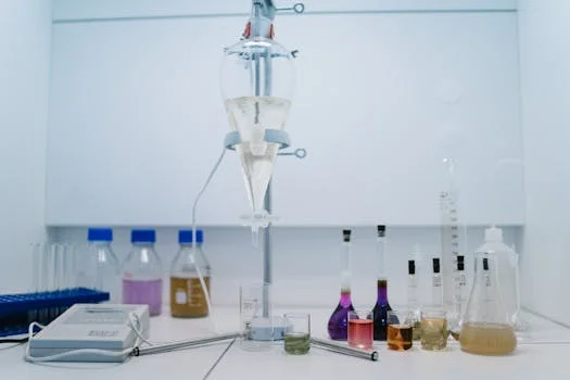
Incomplete fluoride precipitation due to pH drift (actual 7.5–8.0 vs. target 8.5–9.5) is a common pitfall leading to non-compliance in third-generation semiconductor wastewater treatment, often resulting in discharge exceedances. Proactive engineering and operational adjustments are essential to mitigate these risks.
- Pitfall 1: Incomplete Fluoride Precipitation. Achieving the stringent fluoride limits requires precise pH control. If the pH drifts below the optimal 8.5–9.5 range, calcium fluoride (CaF₂) precipitation becomes inefficient, leading to elevated discharge levels.
- Solution: Install robust, multi-point pH probes with an automatic chemical dosing system for lime or caustic soda, ensuring real-time adjustment and maintaining the target pH range for optimal CaF₂ formation.
- Pitfall 2: Arsenic Breakthrough from Co-precipitation Interference. High concentrations of organics or phosphates in the wastewater can interfere with arsenic co-precipitation by competing for binding sites on ferric hydroxide flocs, causing arsenic to pass through the treatment system.
- Solution: Implement a pre-oxidation step using hydrogen peroxide (H₂O₂) or permanganate to convert As(III) to the more easily precipitable As(V), followed by precise ferric chloride (FeCl₃) dosing at pH 6–7.
- Pitfall 3: Membrane Fouling from Colloidal Silica. SiC wastewater often contains high levels of colloidal silica, which can rapidly foul MBR and RO membranes, reducing flux and increasing cleaning frequency and costs.
- Solution: Utilize ultrafiltration (UF) as a dedicated pretreatment stage before MBR/RO, or incorporate silica-specific antiscalants (e.g., polyacrylic acid) and optimize membrane cleaning protocols.
- Pitfall 4: Heavy Metal Exceedances from Inconsistent Sulfide Dosing. Inconsistent or insufficient dosing of sulfide reagents (e.g., Na₂S) for heavy metal precipitation can lead to variable removal efficiencies and discharge exceedances.
- Solution: Integrate online Oxidation-Reduction Potential (ORP) meters to control Na₂S addition, targeting an ORP range of -200 to -300 mV to ensure optimal sulfide availability for metal precipitation.
- Pitfall 5: ZLD System Downtime from Evaporator Scaling. Concentrating brine in evaporators can lead to severe scaling from sparingly soluble salts like calcium sulfate and silica, causing reduced heat transfer efficiency and frequent downtime.
- Solution: Install effective softening pretreatment, such as weak acid cation exchange, prior to the evaporator. Additionally, employ crystallizer seed crystals to promote controlled precipitation of scale-forming compounds.
Frequently Asked Questions
The primary distinction between China GB 8978-2024 and EPA semiconductor wastewater limits lies in fluoride stringency, with EPA’s 4 mg/L being 2.5 times stricter than China’s 10 mg/L.
- What is the biggest difference between China GB 8978-2024 and EPA semiconductor wastewater limits?
China’s fluoride limit (10 mg/L) is 2.5x higher than EPA’s (4 mg/L) for direct discharge, making EPA’s standard more challenging for fluoride removal. However, China’s arsenic limit (0.1 mg/L) is less strict than the EU’s (0.05 mg/L). Both regulatory frameworks increasingly push for Zero Liquid Discharge (ZLD) for high-contaminant fabs to ensure comprehensive compliance. - How do I remove arsenic to <0.05 mg/L for EU compliance?
Achieving arsenic levels below 0.05 mg/L typically requires a two-stage process. First, pre-oxidation with hydrogen peroxide (H₂O₂) or potassium permanganate converts less reactive As(III) to more easily precipitable As(V). Second, co-precipitation with ferric chloride (FeCl₃) at a controlled pH of 6–7 is performed. This is then followed by advanced polishing stages like MBR or RO. For residual arsenic, specialized ion exchange resins, particularly those with iron oxide media, can effectively sorb arsenic down to ultra-low concentrations. - What is the most cost-effective way to meet fluoride limits for a small GaN fab (10 m³/h)?
For smaller flow rates, a chemical precipitation system followed by dissolved air flotation (DAF) can be more cost-effective than a full ZLD system, with a CAPEX typically ranging from $200K–$400K. This approach focuses on efficient calcium fluoride (CaF₂) precipitation. Crucially, ensure the pH is tightly controlled between 8.5–9.5 to maximize CaF₂ removal and minimize the generation of fine, difficult-to-settle particles. However, this system will require regular offsite disposal of fluoride-rich sludge, which can be a significant ongoing OPEX. - Can I reuse ZLD-treated water in my fab’s ultrapure water (UPW) system?
Yes, ZLD-treated water can be reused in a fab’s ultrapure water (UPW) system, but it requires additional, rigorous polishing to meet UPW specifications. The RO permeate from a ZLD system must typically undergo further treatment with ion exchange (e.g., mixed-bed deionizers or electrodeionization, EDI) to remove trace ions down to ppb levels. Additionally, total organic carbon (TOC) must be reduced to below 50 ppb, often through UV oxidation or activated carbon filtration. Most fabs choose to blend ZLD-recovered water with fresh UPW feed to mitigate any residual risk and ensure consistent UPW quality. - What are the penalties for exceeding third-gen semiconductor wastewater limits in China?
Under China’s Water Pollution Prevention Law, penalties for exceeding wastewater discharge limits are severe, with fines ranging from ¥100K–¥1M ($14K–$140K USD) for violations. Repeat offenses or severe environmental damage can lead to production halts, facility closures, and even criminal charges for responsible personnel. Consequently, environmental enforcement is becoming increasingly strict, with ZLD systems increasingly mandated for new third-generation semiconductor fabs, particularly in heavily industrialized regions like Jiangsu and Guangdong provinces, to ensure zero environmental impact.
Further Reading

Explore these in-depth articles on related wastewater treatment topics: