Semiconductor grinding wastewater—generated during silicon wafer backgrinding and dicing—contains ultra-fine silicon particles (<150 nm), heavy metals (copper, nickel), and organic residues that conventional treatment systems (e.g., coagulation + sedimentation) fail to remove efficiently. Advanced ceramic ultrafiltration (UF) membranes (0.1 μm pore size) achieve 99%+ TSS removal without chemical flocculants, while integrated ion exchange and reverse osmosis (RO) systems enable 95% water recovery for reuse. For zero-liquid-discharge (ZLD) compliance, hybrid systems combining UF, RO, and evaporation can reduce wastewater volumes by 99%, cutting fab water costs by up to $0.50/m³ and avoiding regulatory fines of $25,000–$100,000/year per fab.
Why Semiconductor Grinding Wastewater Demands Specialized Treatment
Semiconductor grinding wastewater contains 5,000–50,000 mg/L of total suspended solids (TSS), with approximately 90% of these particles smaller than 150 nm. This sub-micron particle distribution makes traditional gravity-based sedimentation ineffective, as the settling velocity of such fine silicon particles is negligible.Beyond suspended solids, the presence of heavy metals and organic surfactants complicates the waste stream. Chemical Mechanical Polishing (CMP) slurries and etching residues often contribute copper, nickel, and chromium. Under 2024 EPA guidelines, discharge limits for copper are typically restricted to <0.5 mg/L, while nickel must remain <1.0 mg/L. Organic contaminants, including glycols and surfactants used in cleaning steps, can elevate Chemical Oxygen Demand (COD) to ranges between 200 and 1,500 mg/L. If these organics are not addressed, they form a bio-layer on membrane surfaces, drastically reducing flux rates.
Conventional treatment methods, such as basic coagulation and sedimentation, typically achieve only 70–85% TSS removal in these applications. A study by UKM Malaysia noted that standard polymeric filtration systems often experience a 15% flux drop in just 100 minutes of operation when treating grinding wastewater due to the abrasive nature of silicon particles. This necessitates frequent chemical dosing and manual filter changes, increasing operational overhead. Specialized treatment is required to handle the high turbidity and abrasive characteristics of the waste while ensuring copper recovery from semiconductor wastewater meets environmental standards.
| Parameter | Typical Influent (Grinding/Dicing) | Regulatory Limit (Typical) | Removal Requirement |
|---|---|---|---|
| TSS (mg/L) | 5,000 – 50,000 | < 10 – 50 | > 99.9% |
| Particle Size (d90) | < 150 nm | N/A | Sub-micron capture |
| Copper (Cu) | 5.0 – 50.0 mg/L | < 0.5 mg/L | > 99% |
| Nickel (Ni) | 1.0 – 10.0 mg/L | < 1.0 mg/L | > 90% |
| COD | 200 – 1,500 mg/L | < 100 mg/L | > 90% |
Treatment Process Flow: From Grinding Wastewater to Reuse or ZLD
The treatment of semiconductor grinding wastewater requires a multi-stage engineering approach.The process begins with Step 1: Pre-treatment, utilizing rotary drum screens or DAF systems to remove coarse solids (>100 μm) and residual oils. For example, a GX Series Bar Screen with 1–6 mm spacing can remove up to 95% of larger debris, protecting downstream membranes from mechanical damage.
Step 2: Primary Filtration involves the use of ultrafiltration (UF). For grinding wastewater, ceramic UF membranes with a 0.1 μm pore size are preferred over polymeric alternatives due to their superior abrasion resistance. While polymeric hollow-fiber membranes (e.g., Pall Microza) are effective for lower-solids CMP streams, the high TSS of backgrinding waste often leads to fiber breakage. Ceramic modules, such as the Nanostone CM-151, maintain a stable flux of 150–250 LMH (liters per square meter per hour) even under high solids loading, ensuring 99%+ TSS removal.
Step 3: Heavy Metal Polishing is essential for compliance and potential resource recovery. Following UF, the permeate—which is now clear of suspended solids—is passed through chelating ion exchange resins. This step specifically targets dissolved copper and nickel. Copper recovery via ion exchange can often pay for the resin replacement costs over time. If metal concentrations are exceptionally high, chemical precipitation at a pH of 9.0–10.0 may be employed prior to UF.
Step 4: Desalination and Reuse utilizes RO systems for semiconductor water recovery. For grinding wastewater, RO recovery rates typically range from 75–90%. The RO permeate can be recycled back to the cooling towers or used as feed for the Ultrapure Water (UPW) system, while the concentrate is sent to the final stage. Step 5: Zero Liquid Discharge (ZLD) involves thermal evaporation or membrane distillation to treat the RO brine. This results in a solid crystal byproduct and distilled water, achieving a ZLD process design for semiconductor fabs that recovers up to 99% of total influent volume.
Ceramic vs. Polymeric Membranes: Performance, Cost, and Lifespan Comparison
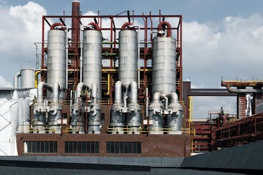
Ceramic membranes, composed of alumina or silicon carbide, possess a Mohs hardness that exceeds that of the silicon particles, allowing for aggressive backwashing and high-pressure crossflow without structural degradation.
From a performance standpoint, ceramic membranes maintain a higher "critical flux." In semiconductor applications, ceramic UF can operate at 200 LMH with a 95% flux recovery after a simple hydraulic backwash. In contrast, polymeric membranes often require frequent chemically enhanced backwashes (CEB) to maintain a flux of 60–80 LMH. While the initial CAPEX for ceramic systems is 2–3 times higher ($500–$1,200/m² vs. $200–$600/m² for polymeric), the total cost of ownership is often lower due to reduced membrane replacement frequency and lower chemical consumption.
The choice between these technologies often depends on the specific waste stream. For backgrinding and dicing wastewater with TSS >1,000 mg/L, ceramic ultrafiltration membranes for semiconductor wastewater are the industry standard. For dilute CMP rinse water with lower solids, polymeric membranes may be more cost-effective. The following table provides a technical head-to-head comparison based on 2025 field data.
| Feature | Ceramic UF (e.g., Alumina/SiC) | Polymeric UF (e.g., PVDF) |
|---|---|---|
| Pore Size | 0.1 μm | 0.01 – 0.1 μm |
| Design Flux | 150 – 300 LMH | 40 – 100 LMH |
| Lifespan | 5 – 10 Years | 3 – 5 Years |
| Abrasion Resistance | Excellent (High Mohs Hardness) | Poor (Prone to fiber breakage) |
| Chemical Resistance | pH 0 – 14 | pH 2 – 11 (typical) |
| CAPEX | High ($$$) | Moderate ($$) |
| OPEX (Cleaning/Power) | Low ($0.05 – $0.10/m³) | Moderate ($0.10 – $0.20/m³) |
Cost Breakdown: CAPEX, OPEX, and ROI for Semiconductor Grinding Wastewater Systems
Capital expenditure (CAPEX) for a 100 m³/h semiconductor wastewater treatment system typically ranges from $1.2M to $5M.Operational expenditure (OPEX) is primarily driven by energy consumption and membrane replacement. A standard UF+RO system operates at approximately $0.30–$0.80/m³, whereas a ZLD system's OPEX jumps to $1.00–$2.50/m³ due to the thermal energy required for evaporation. However, these costs are often offset by significant ROI drivers. With industrial water costs in semiconductor hubs rising to $2.00/m³ or more, a 95% recovery rate can save a large fab over $1M annually in water procurement alone. avoiding regulatory fines—which can range from $25,000 to $100,000 per violation—provides an immediate "insurance" value to the investment.
The payback period for these systems varies by fab size and local utility rates. A 50 m³/h UF+RO system typically sees a return on investment within 2 to 5 years. For ZLD systems, the payback is longer, usually 5 to 10 years, but it is often a mandatory requirement for securing operating permits in water-stressed regions. For a more granular analysis, engineers should consult a detailed cost breakdown for semiconductor wastewater systems to account for local labor and chemical pricing.
| System Type | Capacity | Est. CAPEX | Est. OPEX | Payback Period |
|---|---|---|---|---|
| UF + RO (Reuse) | 50 m³/h | $1.2M – $1.8M | $0.40/m³ | 3 – 4 Years |
| UF + RO (Reuse) | 200 m³/h | $3.5M – $5.0M | $0.32/m³ | 2 – 3 Years |
| Full ZLD System | 50 m³/h | $5.0M – $7.0M | $1.80/m³ | 7 – 9 Years |
| Full ZLD System | 200 m³/h | $12M – $15M | $1.40/m³ | 5 – 7 Years |
ZLD Process Design: How to Achieve 99% Water Recovery in Semiconductor Fabs
Energy optimization is the primary challenge in ZLD design. Modern fabs utilize heat integration, where waste heat from the fab's HVAC or process cooling systems is