Wafer Fab Wastewater Resource Recovery: 2026 Hybrid ZLD Engineering Specs, Fluoride & Silica Removal >99%, $2.8M–$12M CAPEX Breakdown
Wafer fabrication generates 10 m³ of wastewater per 12-inch wafer (DuPont, 2023), with local scrubber streams often containing >50 ppm fluoride and high silica from hydrofluoric acid (HF) cleaning. Hybrid Zero Liquid Discharge (ZLD) systems combining dissolved air flotation (DAF), reverse osmosis (RO), and membrane bioreactors (MBR) achieve >99% removal of fluoride and silica while recovering 85–95% of water for reuse. Capital expenditure (CAPEX) for these systems ranges from $2.8M for small fabs (1–2 million gallons per day, mgd) to $12M for large campuses (10+ mgd), with operational expenditure (OPEX) significantly influenced by membrane replacement, accounting for 30–40% of annual costs.Why Wafer Fabs Are Racing to Adopt ZLD Wastewater Systems
Semiconductor fabs are rapidly implementing ZLD wastewater systems due to escalating water scarcity, stringent environmental regulations, and significant economic incentives. The average semiconductor fab requires between 5 and 10 million gallons per day (mgd) of freshwater to enable wafer production for a single facility, with ultra-pure water (UPW) reject streams accounting for 60–70% of total wastewater volume (IEEE, 2022). This immense water footprint, coupled with regional water stress, compels fabs to prioritize water reuse. The U.S. CHIPS Act incentivizes domestic semiconductor manufacturing, but new fabs established under this initiative face increasingly stricter total dissolved solids (TDS) discharge limits, such as <500 mg/L in California, directly driving the adoption of ZLD solutions to control `TDS control in semiconductor fabs`. Beyond compliance, `water reuse in semiconductor manufacturing` offers substantial cost savings. A semiconductor fabricator in Singapore, for instance, reduced its freshwater intake by 40% by reclaiming local scrubber wastewater with an Electrodialysis Reversal (EDR) system (Veolia, 2021). However, modern hybrid DAF-RO-MBR systems now offer even higher water recovery rates, typically ranging from 85–95%. the semiconductor industry faces a significant 'water-energy nexus'; approximately 1 kWh of electricity consumption requires 2–3 gallons of water for cooling and process support. By recovering and reusing water, fabs achieve a double cost saving: reducing freshwater procurement and minimizing energy expenditure associated with new water treatment. This integrated approach to `semiconductor wastewater ZLD` not only mitigates environmental impact but also enhances operational resilience and financial performance.Wafer Fab Wastewater Streams: Contaminant Profiles and Treatment Challenges
| Wastewater Stream | pH Range | Key Pollutants | Typical Concentrations | Primary Treatment Challenge |
|---|---|---|---|---|
| Local Scrubber | 2.0–6.0 | Fluoride, Silica, Acids | Fluoride: 50–200 ppm Silica: 100–500 ppm |
Fluoride/Silica precipitation, biological fouling |
| CMP | 6.0–9.0 | TSS, Copper, Organic solvents, Abrasives | TSS: 500–2,000 mg/L Copper: 5–50 ppm |
High TSS removal, heavy metal recovery |
| UPW Reject | 6.5–7.5 | TDS (salts from IX regeneration) | TDS: 1,000–5,000 mg/L | Desalination, `TDS control in semiconductor fabs` |
Hybrid ZLD System Design: DAF-RO-MBR Engineering Specs for Wafer Fabs
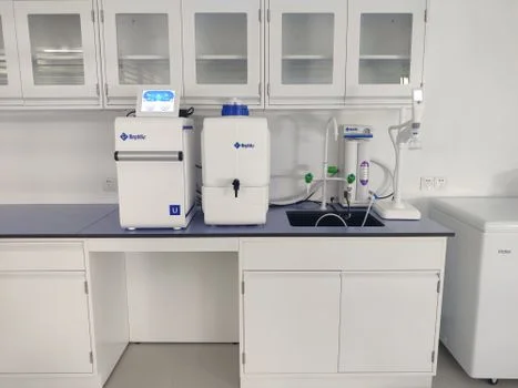
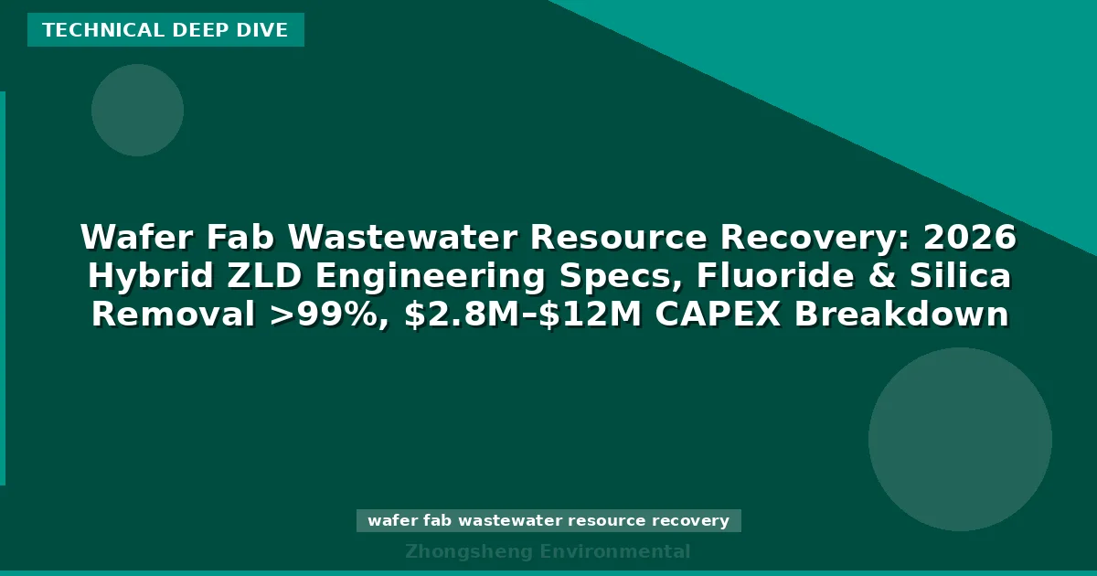
A robust hybrid ZLD system for wafer fabs integrates multiple advanced treatment technologies to achieve high water recovery and contaminant removal. The typical process flow for a DAF-RO-MBR system designed for `wafer fab wastewater resource recovery` includes pretreatment, desalination, biological treatment, and final polishing. The process begins with **Pretreatment**, primarily using Dissolved Air Flotation (DAF) for the removal of total suspended solids (TSS), oils, grease (FOG), and precipitated heavy metals/fluoride. This stage is critical for protecting downstream membrane processes. Zhongsheng Environmental's ZSQ series DAF systems for silica and TSS removal in wafer fab wastewater are engineered to achieve 92–97% TSS removal at flow rates ranging from 4–300 m³/h, with automatic skimming capabilities essential for silica-rich streams. Following DAF, pH adjustment and filtration may be employed to further prepare the water for RO. Next, **Reverse Osmosis (RO)** systems are deployed for `TDS control in semiconductor fabs` and desalination. Industrial RO systems are capable of recovering 75–90% of the water, achieving TDS rejection rates greater than 98%. For an influent TDS concentration of 2,000–5,000 mg/L (typical for UPW reject or pre-treated scrubber/CMP streams), the RO effluent can achieve TDS levels below 100 mg/L. `RO membrane fouling prevention` is paramount, especially considering the presence of silica. Silica scaling in RO membranes requires careful management, including the use of antiscalants (e.g., polyacrylic acid) and precise pH adjustment, typically maintained between 6.5–7.5, to keep silica in a soluble form. The **Membrane Bioreactor (MBR)** stage provides advanced biological treatment, particularly effective for removing organic contaminants (COD) and addressing biological fouling risks. Zhongsheng Environmental's DF series MBR membranes for biological treatment of wafer fab wastewater, featuring 0.1 μm flat-sheet membranes, are designed to handle influent chemical oxygen demand (COD) ranging from 500–2,000 mg/L, producing an effluent with COD consistently below 50 mg/L and TSS below 5 mg/L. This high-quality effluent is suitable for further polishing or direct reuse in less critical applications. Finally, **Polishing** steps, such as ion exchange (IX) or electrodeionization (EDI), are used to achieve the ultra-pure water quality required for specific fab processes, completing the ZLD loop for `water reuse in semiconductor manufacturing`. Here is a typical influent vs. effluent quality table for a hybrid DAF-RO-MBR system:| Parameter | Raw Wastewater (Mixed) | DAF Effluent | RO Permeate | MBR Effluent (Post-RO) | Overall Removal Efficiency |
|---|---|---|---|---|---|
| TSS (mg/L) | 500–2,000 | 30–150 | <5 (if fed to RO) | <5 | >99% |
| COD (mg/L) | 500–2,000 | 100–500 | <50 (if fed to RO) | <50 | >97% |
| TDS (mg/L) | 1,000–5,000 | 1,000–5,000 | <100 | <100 | >98% |
| Fluoride (ppm) | 50–200 | <10 (post-precipitation) | <0.5 | <0.5 | >99% |
| Silica (ppm) | 100–500 | <50 (post-coagulation) | <5 | <5 | >99% |
$2.8M–$12M CAPEX Breakdown: ZLD System Costs for Small, Medium, and Large Wafer Fabs
| Fab Scale (Wastewater Flow) | Typical CAPEX Range | Key OPEX Drivers (per m³) | Estimated Payback Period |
|---|---|---|---|
| Small (1–2 mgd) | $2.8M–$4.5M | Membranes: $0.50–$1.00 Energy: $0.30–$0.60 Labor: $0.20–$0.40 |
4–5 years |
| Medium (5 mgd) | $6.5M–$8M | Membranes: $0.50–$1.00 Energy: $0.30–$0.60 Labor: $0.20–$0.40 |
3–4 years |
| Large (10+ mgd) | $10M–$12M | Membranes: $0.50–$1.00 Energy: $0.30–$0.60 Labor: $0.20–$0.40 |
3–3.5 years |
How to Select the Right ZLD Technology for Your Wafer Fab’s Wastewater
Selecting the optimal ZLD technology for `wafer fab wastewater resource recovery` requires a systematic decision framework that considers the specific contaminant profile, desired water recovery goals, and economic factors. The choice between hybrid membrane systems, electrodialysis reversal (EDR), or evaporators depends heavily on the wastewater characteristics. A robust decision tree for technology selection begins with the primary contaminants present: 1. Contaminant Profile: Identify whether the dominant pollutants are high TSS and organics (e.g., from CMP), fluoride and silica (from scrubber streams), or primarily high TDS (from UPW reject). 2. Recovery Goals: Determine the desired water reuse rate. Are you aiming for 85% recovery for non-critical uses, or 95%+ for high-purity process water? **Hybrid DAF-RO-MBR systems** are best suited for comprehensive `semiconductor wastewater ZLD` when the wastewater contains a mix of high TSS (e.g., CMP streams), significant fluoride and silica (e.g., scrubber streams), and moderate TDS (1,000–5,000 mg/L). This combination offers high removal efficiencies for diverse pollutants and achieves high water recovery (85–95%) at a competitive OPEX, making it ideal for `HF wastewater treatment` and `silica removal in wafer fabs`. For a deeper dive into these systems, refer to our 2027 engineering specs for silicon wafer wastewater treatment. **Electrodialysis Reversal (EDR)** is a strong contender for streams with high TDS (5,000–10,000 mg/L) that require desalination, particularly when chloride salts are predominant. However, EDR systems typically struggle with high silica concentrations and require effective pretreatment to prevent scaling. **Evaporators and Crystallizers** are generally reserved for highly concentrated brine streams with TDS exceeding 10,000 mg/L, where other technologies become economically unfeasible. While they achieve true ZLD (producing solid waste), their primary drawback is very high energy consumption, with OPEX typically ranging from $0.80–$1.50 per cubic meter of treated water, making them the most expensive option for bulk water treatment. The table below provides a comparison of these key ZLD technologies:| Technology | Best For (Contaminant Profile) | Typical Recovery Rate | Relative CAPEX | Relative OPEX | Key Limitation |
|---|---|---|---|---|---|
| Hybrid DAF-RO-MBR | High TSS, Fluoride, Silica, Moderate TDS (1K-5K mg/L) | 85–95% | Medium | Medium | Requires robust `RO membrane fouling prevention` |
| Electrodialysis Reversal (EDR) | High TDS (5K-10K mg/L), especially chlorides | 80–90% | Medium-High | Medium | Sensitive to silica, organics; requires extensive pretreatment |
| Evaporators/Crystallizers | Very High TDS (>10K mg/L), Brine concentration | 95–99% (to solid) | High | Very High (energy-intensive) | Highest energy cost, complex operation |
Frequently Asked Questions